Method and apparatus for producing uniform processing rates

Inactive Publication Date: 2005-01-11
LAM RES CORP
View PDF13 Cites 14 Cited by
  • Summary
  • Abstract
  • Description
  • Claims
  • Application Information

AI Technical Summary

Benefits of technology

According to a further aspect of the invention there is provided a method for improving plasma processing uniformity in a plasma processing device. An antenna arrangement generates an rf field distribution inside the plasma processing device, and includes an rf inductive antenna connected to an rf power supply to supply an rf current to generate a first rf field extending into the plasma generating region and a passive antenna configured to generate a second rf field. The method comprises the steps of inductively coupling the passive antenna and the rf inductive antenna. The passive ante

Problems solved by technology

One problem that has been encountered with inductive plasma systems, such as the one mentioned above, has been variations in the etch performance across the substrate, e.g., a non-uniform etch rate.
As a result, it is extremely difficult to control the parameters associated with a work piece, e.g., critical dimensions, aspect ratios, and the like in the case of integrated circuits.
Additionally, a non-uniform etch rate may lead to device failure in the semiconductor circuit, which typically translates into higher costs for the manufacturer.
Moreover, there also exist other issues of concern such as the overall etch rate, etch profile, micro-loading, selectivity, and the like.
However, the requirement of providing rf power feeds means that the antenna cannot be perfectly azimuthally symmetric.
Normal

Method used


Image

  • Method and apparatus for producing uniform processing rates
  • Method and apparatus for producing uniform processing rates
  • Method and apparatus for producing uniform processing rates

Examples


Embodiment Construction

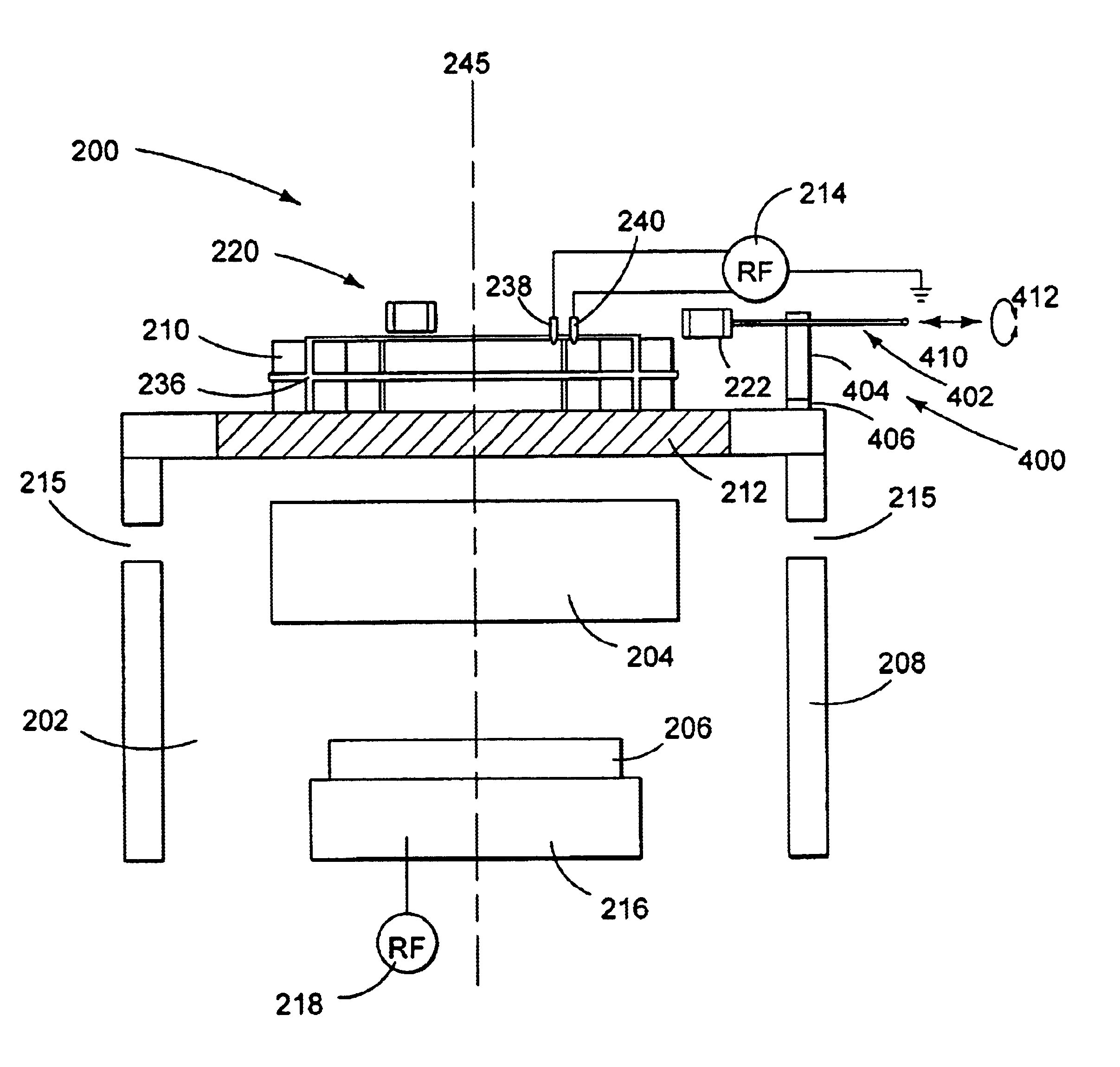
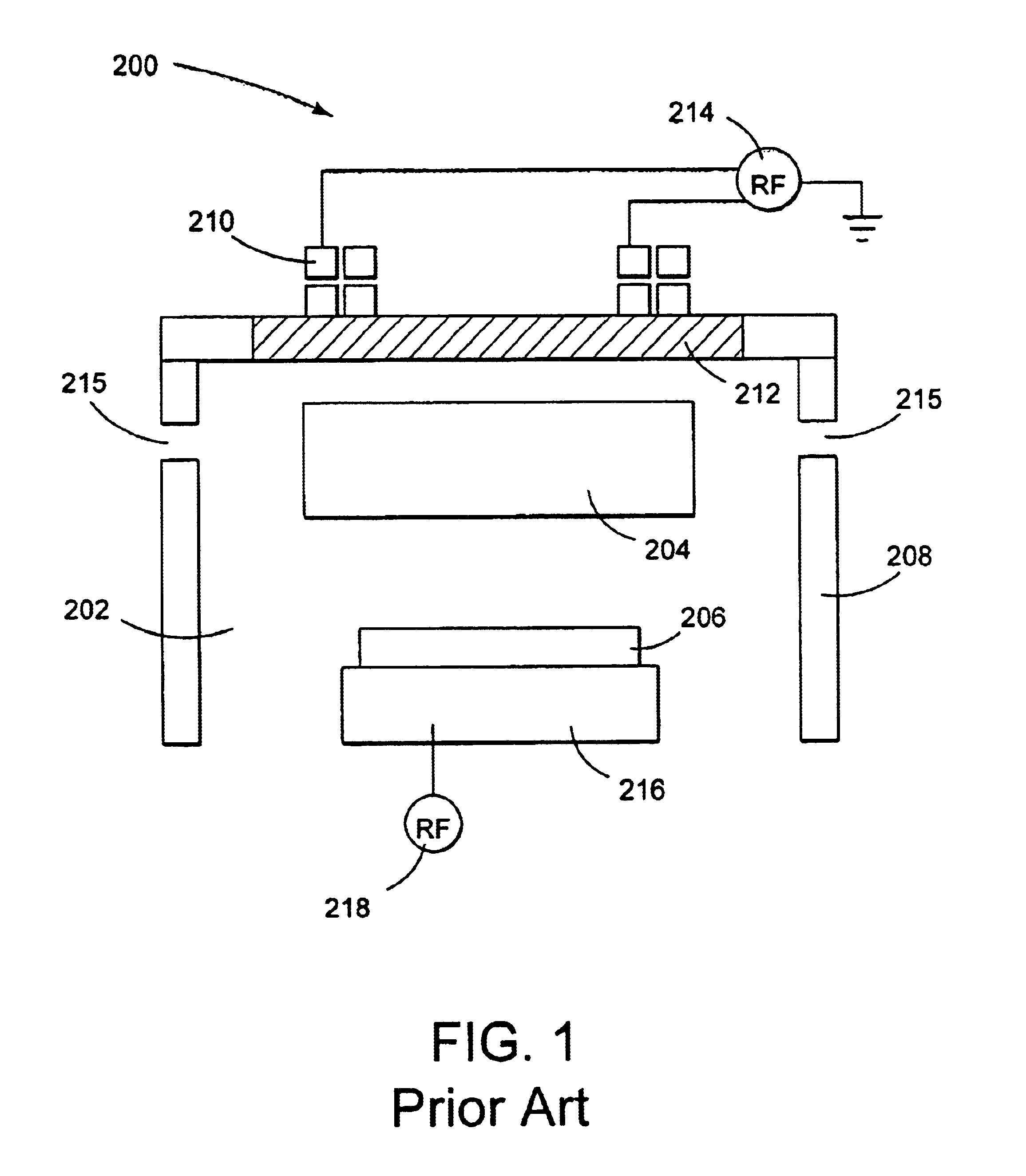
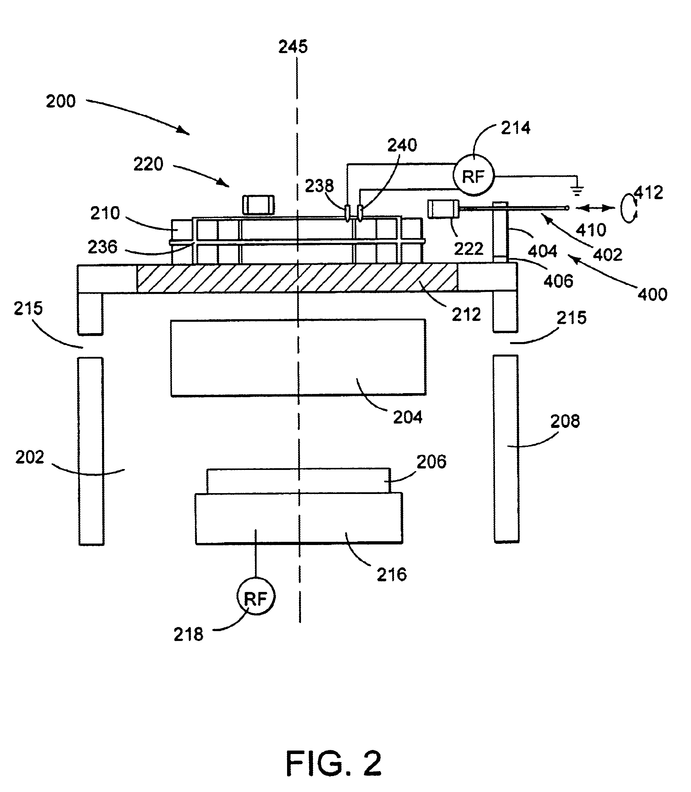
The present invention relates to methods and apparatus for increasing processing uniformity across a workpiece in a plasma processing device or tool. FIG. 1 shows a prior art plasma processing device as discussed above. The device includes an inductive rf antenna 210 connected to an rf power supply which provides a source of rf current to the antenna. In simple terms, the rf antenna generates an rf electromagnetic field distribution in a plasma processing region in the processing chamber 202 which ignites and sustains a plasma 204.

There is an rf voltage on the rf antenna and an rf current in the rf antenna. The rf voltage varies along the length of the antenna and the largest voltage difference is typically from one end (i.e. terminal) to the other end (i.e. terminal). The largest voltage difference can typically be of order several thousand volts. Both the rf voltage on the rf antenna and the rf current in the rf antenna can affect the plasma.

The rf voltage on the rf antenna direct...


PUM

PropertyMeasurementUnit
Lengthaaaaaaaaaa
Magnetic fieldaaaaaaaaaa
Sizeaaaaaaaaaa

Abstract

An antenna arrangement for generating an rf field distribution at a plasma generating region inside a chamber wall of a process chamber of a plasma processing apparatus is described. The antenna arrangement includes an rf inductive antenna to which an rf power supply can be connected to supply an rf current to generate a first rf field extending into the plasma generating region. A passive antenna is also provided which is inductively coupled to the rf inductive antenna and configured to generate a second rf field modifying the first rf field. The rf field distribution at the plasma generating region increases the processing uniformity of the processing apparatus compared to that in the absence of the passive antenna.

Description

BACKGROUND OF THE INVENTIONThe present invention relates generally to apparatus and methods for processing substrates, including semiconductor substrates for use in IC fabrication or glass panels for use in flat panel display applications. More particularly, the present invention relates to improved plasma processing systems that are capable of processing substrates with a high degree of processing uniformity across the substrate surface.Plasma processing systems have been around for some time. Over the years, plasma processing systems utilizing inductively coupled plasma sources, electron cyclotron resonance (ECR) sources, capacitive sources, and the like, have been introduced and employed to various degrees to process various items such as semiconductor substrates and glass panels.During processing, multiple deposition and / or etching steps are typically employed. During deposition, materials are deposited onto a substrate surface (such as the surface of a glass panel or a wafer). ...

Claims


Application Information

Patent Timeline
IPC IPC(8): H01J37/32H01Q1/22H01Q1/26H01Q11/12H01Q11/00H05H1/46H01L21/3065H01Q7/00H01Q21/29
CPCH01J37/321H01J37/3299H05H1/46H01Q21/29H01Q7/00H01L21/3065H01J37/32
Inventor HOWALD, ARTHUR M.KUTHI, ANDRASWILCOXSON, MARK HENRYBAILEY, III, ANDREW D.
Owner LAM RES CORP
Why Eureka
Try Eureka