Semiconductor passive Q-switch providing variable outputs

a technology of q-switching and semiconductors, applied in the direction of laser optical devices, laser details, optics, etc., can solve the problem of limited theoretically achievable shortest pulse duration of q-switching laser systems, inability to control or adjust passive q-switching parameters, and inability to achieve effective transmission of gaas wafers.

Inactive Publication Date: 2005-01-11
NANYANG TECH UNIV
View PDF9 Cites 16 Cited by
  • Summary
  • Abstract
  • Description
  • Claims
  • Application Information

AI Technical Summary

Benefits of technology

The current invention is conceptualized based on this new development. By applying gradient coating on a single piece of GaAs wafer, the effective transmittance of the GaAs wafer can be varied. Therefore, using a single piece of gradient coated GaAs wafer, the laser output characteristics of the GaAs Q-switch, operating at a fixed pump power, can be varied. This improvement avoids the many disadvantages of using pump power as the variable parameter in changing the laser output characteristics.

Problems solved by technology

A major disadvantage of passive Q-switching, as compared to active Q-switching, is non-adjustability of the parameters of the Q-switched pulses.
There is no effective way to control or adjust the parameters of passive Q-switching.
Generally, the theoretically shortest pulse duration achievable from a Q-switched laser system is limited by the round-trip time of the laser cavity.
However, there are disadvantages in using pump power as the control variable as the emission wavelength of the diode laser may drift away from its optimum value, the temperature of the diode laser may take a long time to stabilise, and the beam quality of the Nd:YAG laser output may change substantially.

Method used


Image

  • Semiconductor passive Q-switch providing variable outputs
  • Semiconductor passive Q-switch providing variable outputs
  • Semiconductor passive Q-switch providing variable outputs

Examples


Embodiment Construction

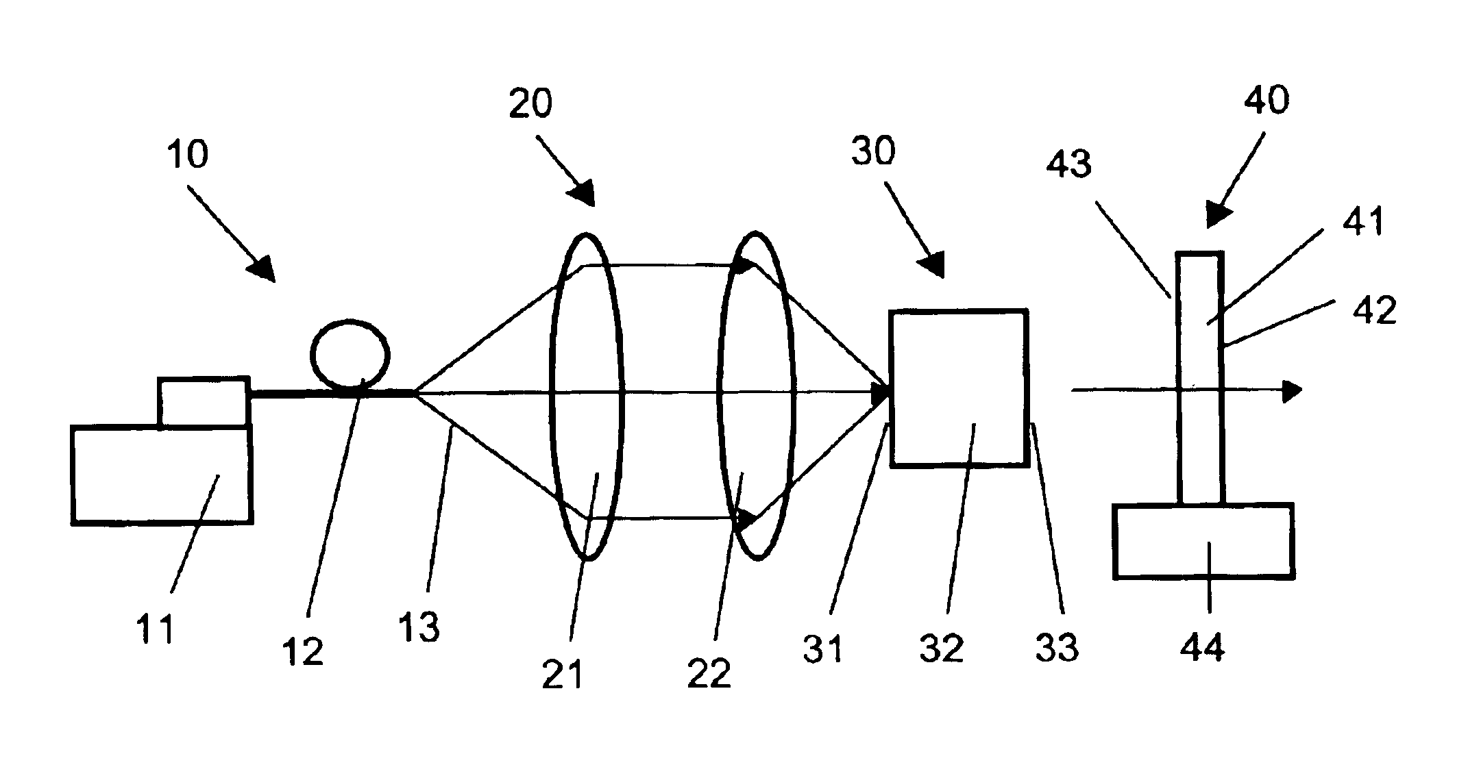
FIG. 1 illustrates schematically the use of a semiconductor wafer in a laser system including a pumping source 10, a beam shaping system 20, a laser gain material 30, and a passive Q-switch 40, which also serves as the output coupler for the laser system. In an alternative embodiment, the tunable passive Q-switch may not operate simultaneously as the output coupler of the laser system. In such a case, in line with common practice in the trade, a partially transmitting mirror at the laser wavelength may be used as the output coupler.

The pumping source 10 consists of a diode laser 11 and delivery optical fiber 12, providing a pumping laser beam 13, which has a center wavelength matching the absorption peak of the laser crystal 32. The laser beam 13 is collimated by a first lens 21 and then focused by a second lens 22 to a laser crystal 32. The laser crystal 32 is 1% (by atomic weight) doped Nd:YVO4, with one facet 31 anti-reflection (AR) coated at the wavelength of 808 nm and high-ref...


PUM

PropertyMeasurementUnit
wavelengthaaaaaaaaaa
widthaaaaaaaaaa

Abstract

A semiconductor wafer with variable transmittance, serves as a saturable absorber for performing passive Q-switching in a laser system to produce laser pulses having defined output characteristics. By translating or rotating the semiconductor saturable absorber, loss properties of a laser cavity may be altered. In this manner, the output characteristics of the laser pulses can be varied without changing other parameters of laser operation. The output characteristics may include pulse duration, pulse repetition rate, peak power and average output power of the laser pulses. The semiconductor wafer can be made of doped or undoped GaAs, AlGaAs, InP, etc. Furthermore, the tunable Q-switch may simultaneously serve as an output coupler for the laser cavity.

Description

TECHNICAL FIELDThis invention relates to passive Q-switching of a laser system. In particular the invention relates to a passive Q-switch that may be used in a laser system to produce laser pulses having variable output characteristics. The Q-switch may include a semiconductor wafer. The output characteristics of the laser pulses may be tuned by changing the transmittance of the wafer. The output characteristics may include pulse duration and pulse repetition rate of the Q-switched laser beam. The same semiconductor wafer may be simultaneously used as the output coupler of the cavity of the laser to render the laser system more compact.BACKGROUND OF THE INVENTION AND PRIOR ARTQ-switching is a common and effective technique to achieve optical pulses with short duration, high repetition rate and high peak power. These characteristics are required for laser ranging, nonlinear studies, medicine, laser micro-machining, and other important applications. Q-switching can be effected using a...

Claims


Application Information

Patent Timeline
Patent Type & Authority Patents(United States)
IPC IPC(8): H01S3/113H01S3/10H01S3/11G02F1/35H01S3/00H01S3/0941H01S3/098H01S3/16
CPCG02F1/3523H01S3/09415H01S3/113H01S3/1118H01S3/005H01S3/1673H01S3/1611
Inventor TAM, SIU CHUNGGU, JIAN HUILAM, YEE LOY
Owner NANYANG TECH UNIV
Why Eureka
Try Eureka