Method and apparatus for fully aligned flip-chip assembly having a variable pitch packaging substrate

a flip-chip and variable pitch technology, applied in the direction of individual semiconductor device testing, semiconductor/solid-state device testing/measurement, instruments, etc., can solve the problems of limiting the programming of die placement currently used in the semiconductor industry, compromising the structural integrity of the chip, unduly limiting the electrical and thermal throughput, etc., to maximize the cross-sectional area of the solder joint, increase the manufacturing yield, and increase the package reliability

Inactive Publication Date: 2005-01-11
GLOBALFOUNDRIES INC
View PDF1 Cites 3 Cited by
  • Summary
  • Abstract
  • Description
  • Claims
  • Application Information

AI Technical Summary

Benefits of technology

An advantage of the present invention includes increasing the package reliability, because the solder material (the solder bump and the package solder) is accurately aligned between both the die pad and the substrate pad, solving the misalignment problem so prevalent in the prior art using packaging substrates which are unable to compensate for any mismatches in the coefficients of thermal expansion. Another advantage of the present invention is that the electrical path is shorter with the present fully aligned assembly as its solder material is also fully aligned. The present assembly, as finally fabricated, allows for symmetrical alignment of the solder bump with the package solder and the substrate pad, thereby maximizing the cross-sectional area of the solder joint which reduces its electrical path resistance well below that of the prior art assemblies. With the present advantages, manufacturing yield is increased as any die misalignment occurring during die placement is compensated by the present preconfigured variable pitch packaging substrate. Other features of the present invention are disclosed, or are apparent in the section entitled “Detailed Description of the Invention.”
includes increasing the package reliability, because the solder material (the solder bump and the package solder) is accurately aligned between both the die pad and the substrate pad, solving the misalignment problem so prevalent in the prior art using packaging substrates which are unable to compensate for any mismatches in the coefficients of thermal expansion. Another advantage of the present invention is that the electrical path is shorter with the present fully aligned assembly as its solder material is also fully aligned. The present assembly, as finally fabricated, allows for symmetrical alignment of the solder bump with the package solder and the substrate pad, thereby maximizing the cross-sectional area of the solder joint which reduces its electrical path resistance well below that of the prior art assemblies. With the present advantages, manufacturing yield is increased as any die misalignment occurring during die placement is compensated by the present preconfigured variable pitch packaging substrate. Other features of the present invention are disclosed, or are apparent in the section entitled “

Problems solved by technology

This being so, the solder bump is usually misaligned while reflowing the package solder element in forming the solder joints in the related art assemblies as the package substrate tends to expand at a rate greater than does the chip, thereby compromising their structural integrity, and thereby unduly limiting their electrical and thermal throughput.
In addition, such misalignment results from the limited die placement programming currently used in the semiconductor industry.
Thus, as the die pitch (i.e., bump to bump centers) decreases, a potential for lower manufacturing yield at the flip-chip attach (FCA) stage exists due to the prior art non-variable substrate pitch configuration and to the limitations of current die placement machine tolerances.

Method used


Image

  • Method and apparatus for fully aligned flip-chip assembly having a variable pitch packaging substrate
  • Method and apparatus for fully aligned flip-chip assembly having a variable pitch packaging substrate
  • Method and apparatus for fully aligned flip-chip assembly having a variable pitch packaging substrate

Examples


Embodiment Construction

.”

BRIEF DESCRIPTION OF THE DRAWINGS

For a better understanding of the present invention, reference is made to the below-referenced accompanying Drawings. Reference numbers refer to the same or equivalent parts of the present invention throughout the several figures of the Drawings.

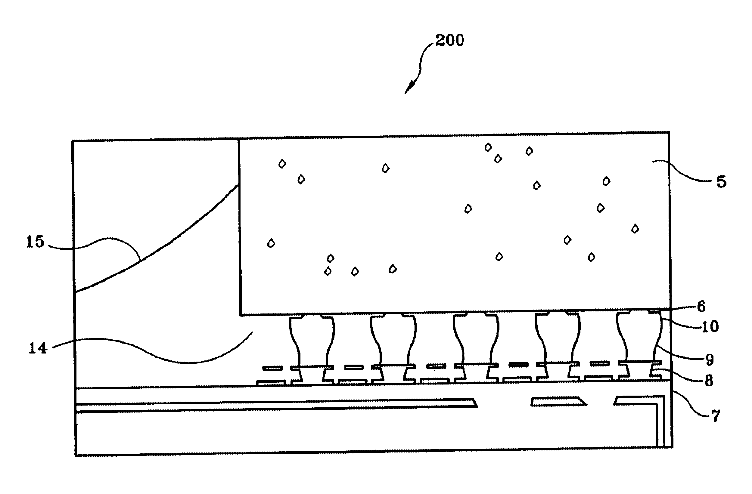
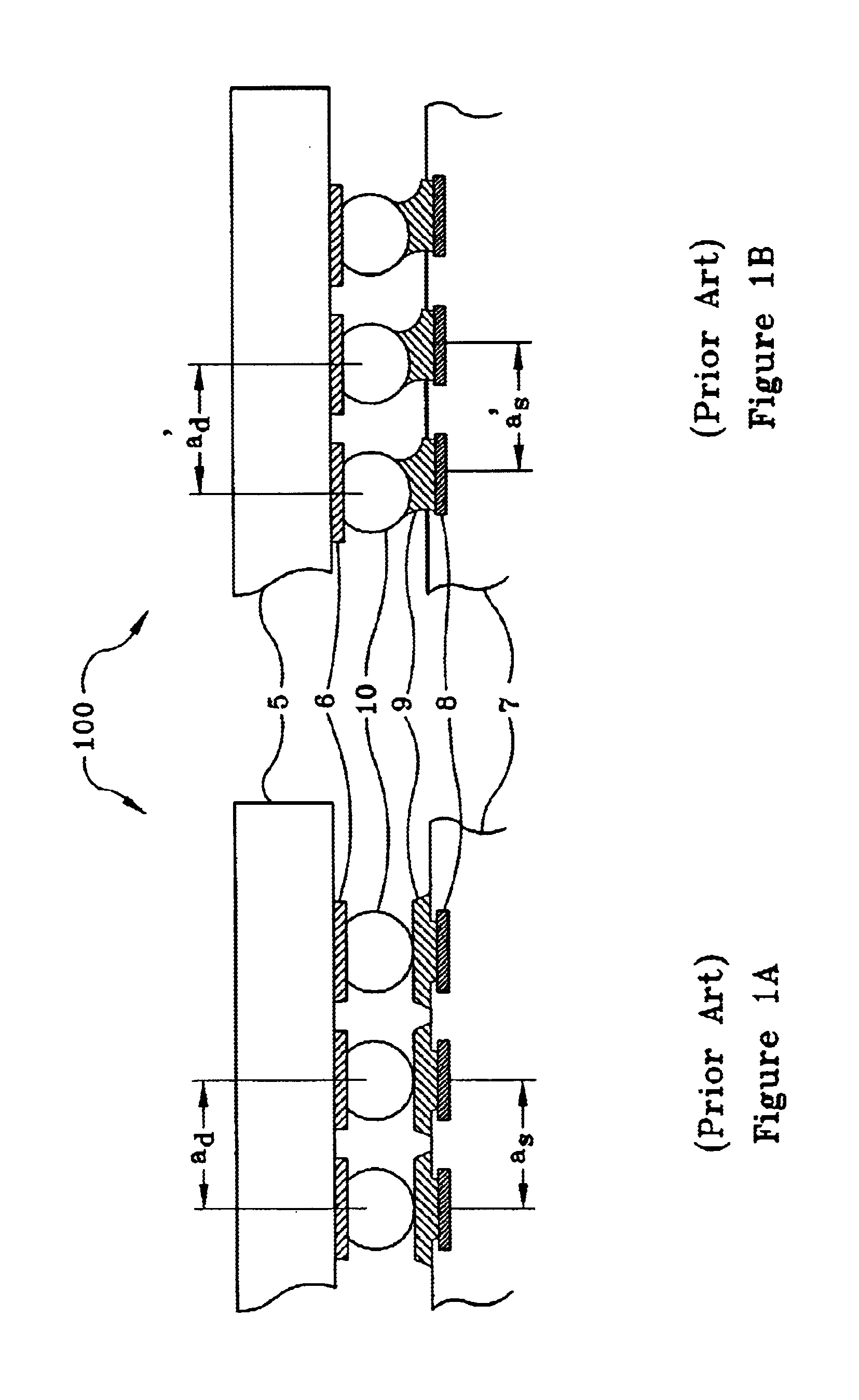
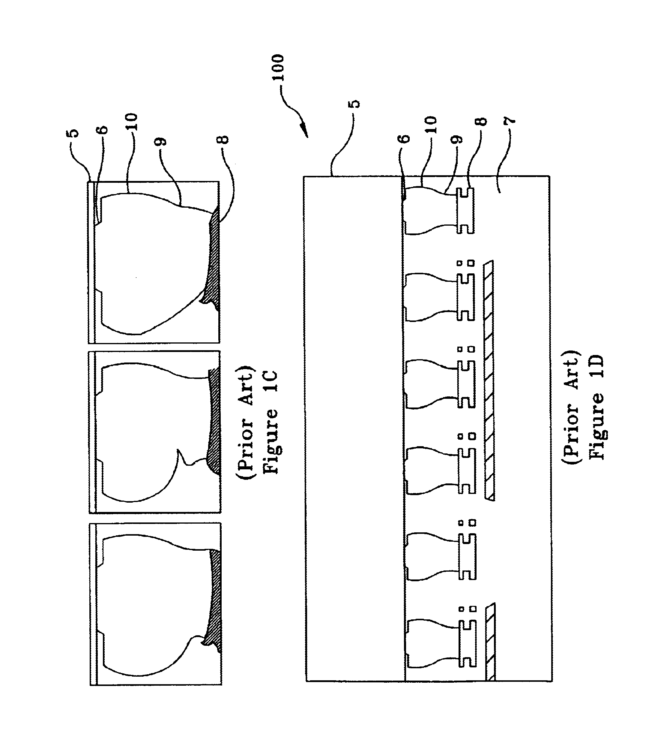
FIG. 1A is a cross-sectional view of a flip-chip assembly, comprising: a die having a plurality of die pads thereon formed with a design die pad pitch value; a package substrate having a plurality of substrate pads thereon formed with a design substrate pad pitch value to match the design die pad pitch value; a corresponding plurality of solder bumps formed on the plurality of die pads; and a corresponding plurality of package solder elements formed on the plurality of substrate pads, wherein the plurality of solder bumps are disposed over the corresponding plurality of package solder elements, prior to a reflow process, in accordance with the prior art.

FIG. 1B is a cross-sectional view of the flip-chip ass...


PUM


Abstract

A method and an apparatus for preventing misalignment of semiconductor packaging assembly materials. In particular, a method of fabricating a fully aligned flip-chip assembly having a variable pitch packaging substrate, involves: providing a set of input data; calculating a set of intermediate data using the input data set; calculating a set of final substrate pad coordinates using the intermediate data set, thereby providing a set of output data; providing a packaging substrate having a plurality of substrate pads thereon formed according to the output data set to compensate for any inchoate thermogeometric hysteresis arising from any mismatched coefficients of thermal expansion, and thereby fabricating the flip-chip assembly having a variable pitch packaging substrate, and an assembly thereby fabricated which is more robust to any temperature-induced stress.

Description

TECHNICAL FIELDThe present invention relates to the assembly and the packaging of semiconductor chips. More particularly, the present invention relates to assembly and the packaging of flip-chips. Even more particularly, the present invention relates to reducing stress in the flip-chip assembly.BACKGROUND ARTCurrently, for chip assemblies, the semiconductor industry has been utilizing solder-bumped flip-chip technology, such as “C4” (controlled-collapse chip connection), wherein solder bumps are formed on a solder-wettable terminal on the chip or die (i.e., wafer bumping) on a die pad which corresponds to a package solder element formed on a solder-wettable terminal on the package substrate (i.e., substrate preparation). The solder joints are formed by reflowing the package solder element onto the solder bump, wherein the other remaining elements of the assembly are subjected to the same heated environment as the package substrate. The chip or die and the substrate, being formed fro...

Claims


Application Information

Patent Timeline
Patent Type & Authority Patents(United States)
IPC IPC(8): H01L21/02H01L21/56H01L23/14H01L23/12
CPCH01L21/563H01L23/145H01L2224/73203
Inventor WEIDLER, JAIME D.NEWMAN, ROBERT A.KWON, JINSU
Owner GLOBALFOUNDRIES INC
Why Eureka
Try Eureka