High permeability composite films to reduce noise in high speed interconnects

a composite film, high-permeability technology, applied in the field of integrated circuits, can solve the problems of reflection and ringing, difficult to achieve larger values, limited switching time of cmos circuits, etc., to achieve high speed, improve and efficiently fabricated techniques, and improve performan

Inactive Publication Date: 2005-01-18
MICRON TECH INC
View PDF43 Cites 46 Cited by
  • Summary
  • Abstract
  • Description
  • Claims
  • Application Information

AI Technical Summary

Benefits of technology

[0017]The above mentioned problems with CMOS line interconnections as well as other problems are addressed by the present invention and will be understood by reading and studying the following specification. High speed interconnections are provided which accord exemplary performance. That is, the invention described here provides an improved and efficiently fabricated technique for high speed transmission lines on CMOS integrated circuits. In addition, the novel low input impedance CMOS circuit offers the following advantages: (1) the signal delay depends only on the velocity of light on the line and is easily predictable and reproducible, eliminating or allowing for compensation for signal and / or clock skew, (2) there are no reflections at the receiving end of the line and this minimizes ringing, and (3) noise signals will be smaller due to weaker coupling between lines resulting in better signal to noise ratios, the noise current will only be a small fraction of the signal current.

Problems solved by technology

Most commonly used coaxial lines have an impedance of 50 ohms or 75 ohms, it is difficult to achieve larger values.
Switching times in CMOS circuits have been limited by the ability to switch the capacitive loads of long lines and buffers, and charge these capacitances over large voltage swings to yield a voltage step signal.
This is problematic in that:
(ii) the line is not terminated by its characteristic impedance resulting in reflections and ringing,
(iii) large noise voltages may be induced on the signal transmission line due to capacitive coupling and large voltage swing switching on adjacent lines, the noise voltage can be a large fraction of the signal voltage.
Long lines result is slow switching speeds and excessive noise due to capacitive coupling between lines.
This is problematic in that the interconnection lines are normally loaded with the capacitive input of the next CMOS stage and the large stray capacitance of the line itself.
The response time is normally slow due to the limited ability of the line drivers to supply the large currents needed to charge these capacitances over large voltage swings.
Furthermore, if two interconnection wires are in close proximity then the voltage swing on one line can induce a large voltage swing or noise voltage on the adjacent line as shown in FIG.

Method used


Image

  • High permeability composite films to reduce noise in high speed interconnects
  • High permeability composite films to reduce noise in high speed interconnects
  • High permeability composite films to reduce noise in high speed interconnects

Examples


Embodiment Construction

[0029]FIG. 9 illustrates another embodiment for a pair of neighboring transmission lines, according to the teachings of the present invention.

[0030]FIG. 10 illustrates another embodiment for a pair of neighboring transmission lines, according to the teachings of the present invention.

[0031]FIG. 11 illustrates another embodiment for a pair of neighboring transmission lines, according to the teachings of the present invention.

[0032]FIG. 12 illustrates another embodiment for a pair of neighboring transmission lines, according to the teachings of the present invention.

[0033]FIG. 13 is a block diagram which illustrates an embodiment of a system using line signaling according to teachings of the present invention.

[0034]FIG. 14 is a block diagram which illustrates another embodiment of a system according to teaching of the present invention.

DETAILED DESCRIPTION

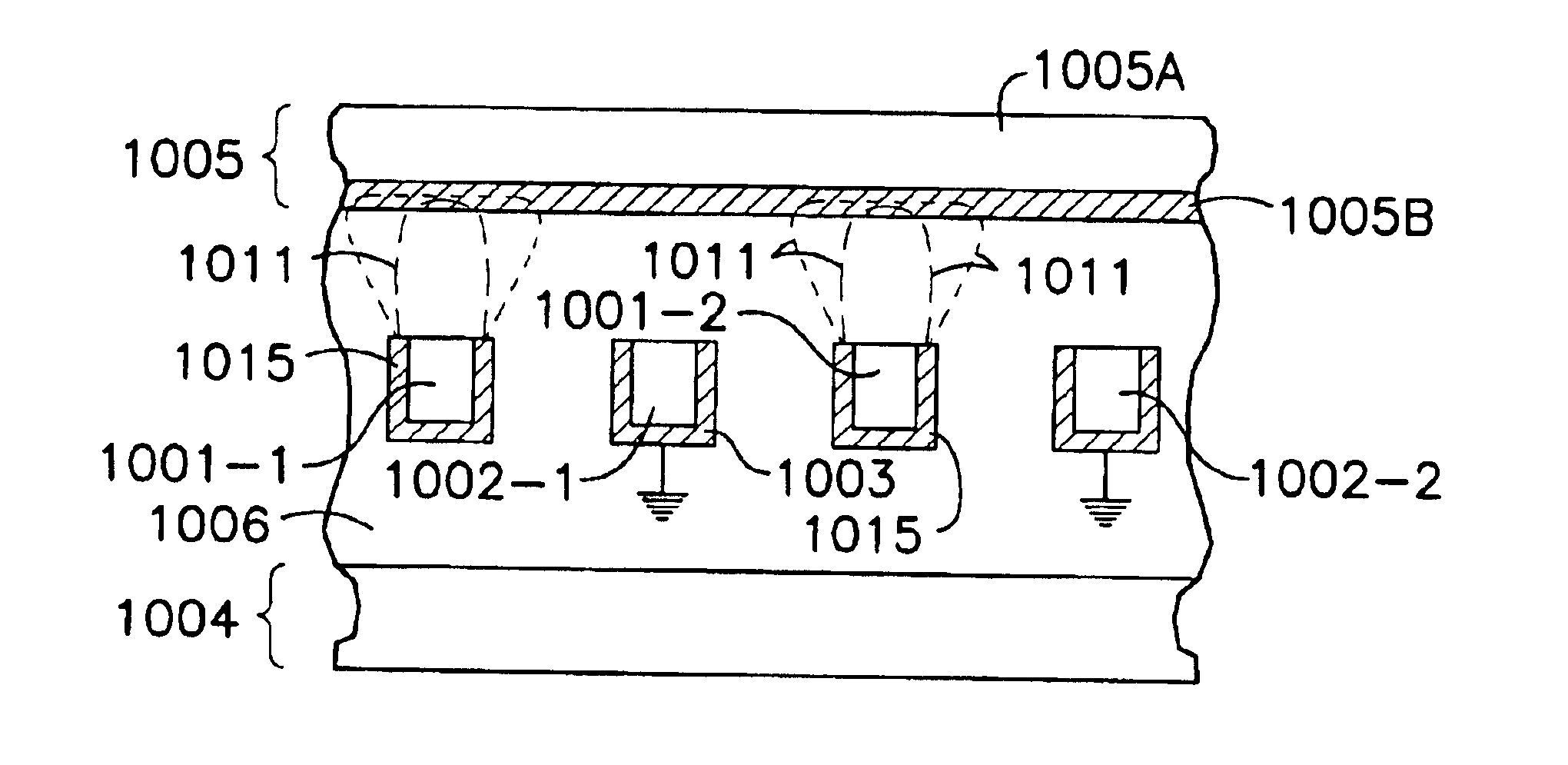
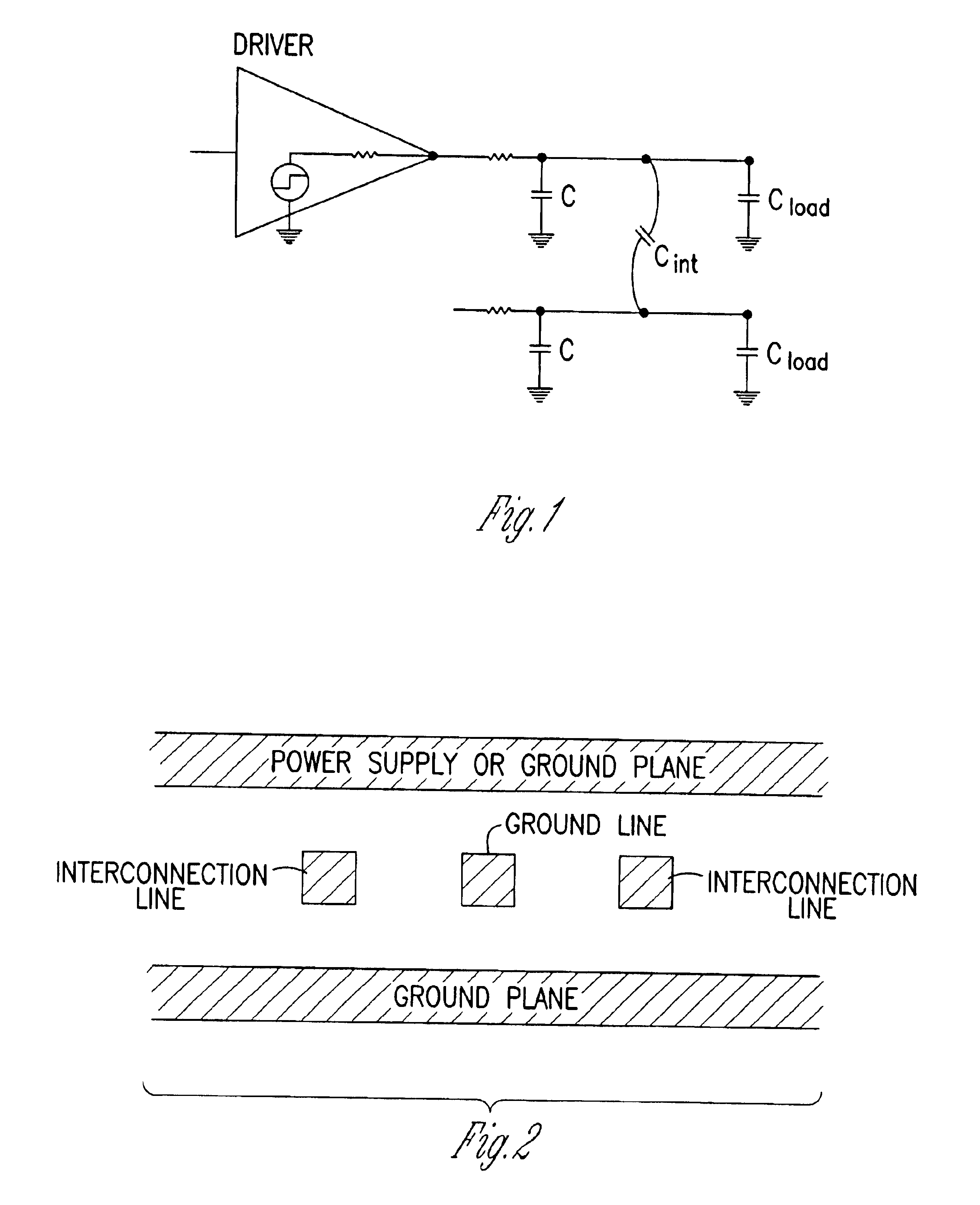
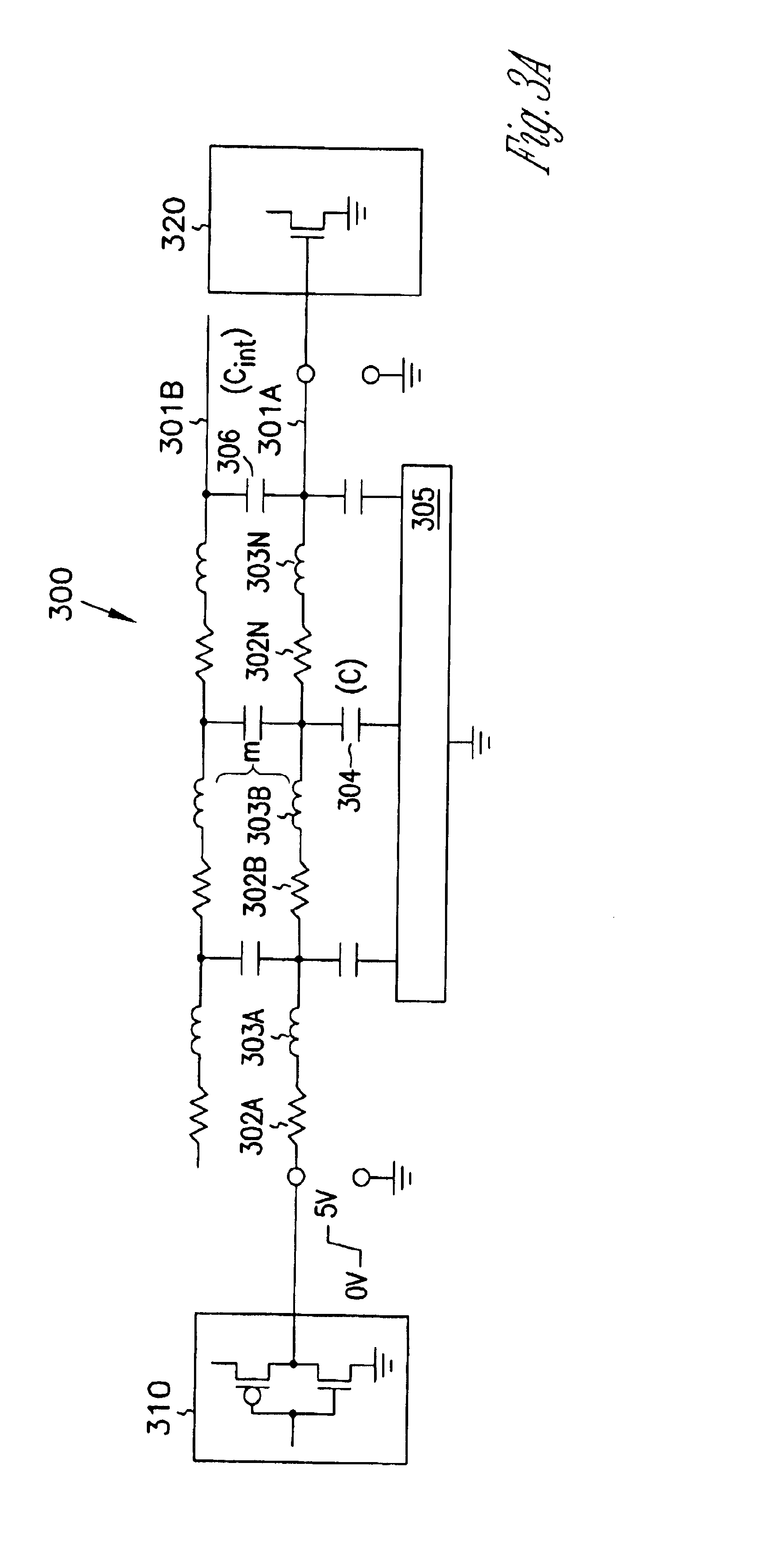
[0035]In the following detailed description of the invention, reference is made to the accompanying drawings which form a part here...


PUM


Abstract

A method for forming integrated circuit lines provides a structure for improved operation on integrated circuits. A method includes forming a first layer of electrically conductive material on a substrate. A first layer of insulating material is formed on the first layer of the electrically conductive material. A number of integrated circuit lines is formed on the first layer of insulating material. A number of conductive lines is formed on the first layer of insulating material between and parallel with the number of intergrated circuit lines, where each conductive line includes a composite ferrite film. A second layer of insulating material is formed on the integrated circuit lines and the conductive lines. The method includes forming a second layer of electrically conductive material on the second layer of insulating material.

Description

RELATED APPLICATION(S)[0002]This application is a Divisional of U.S. application Ser. No. 10 / 099,020 filed on Mar. 13, 2002 which is incorporated herein by reference.FIELD OF THE INVENTION[0003]The present invention relates generally to integrated circuits. More particularly, it pertains to structure and methods for improved transmission line interconnections.BACKGROUND OF THE INVENTION[0004]The metal lines over insulators and ground planes, or metal lines buried in close proximity to dielectric insulators and used for integrated circuit interconnects are in reality transmission lines or strip lines. The use of coaxial interconnection lines for interconnections through the substrate in CMOS integrated circuits can also be termed transmission lines or strip lines. Interconnection lines on interposers or printed circuit boards can also be described as transmission lines.[0005]The low characteristic impedance of any of these lines, transmission, strip lines or coaxial lines results in ...

Claims


Application Information

Patent Timeline
Patent Type & Authority Patents(United States)
IPC IPC(8): G11C7/00G11C7/18H01L23/522H01L23/52
CPCG11C7/02G11C7/18H01L23/5225H01L2223/6627H01L2924/1903H01L2924/0002H01L2924/3011H01L2924/00
Inventor FORBES, LEONARDAHN, KIE Y.AKRAM, SALMAN
Owner MICRON TECH INC
Why Eureka
Try Eureka