Semiconductor device with super junction region

a technology of super junction region and semiconductor device, which is applied in the direction of semiconductor device, basic electric element, electrical apparatus, etc., can solve the problems of device breaking, device with high breakdown voltage disadvantageous in on-state resistance, and no structure developed

Inactive Publication Date: 2005-01-18
KK TOSHIBA
View PDF21 Cites 155 Cited by
  • Summary
  • Abstract
  • Description
  • Claims
  • Application Information

AI Technical Summary

Benefits of technology

a control electrode which is formed on the surface of the first—first conductivity type semiconductor layer sandwiched by the adjacent second—second conductivity type semiconductor layers, the surf...

Problems solved by technology

However, on the other hand, because there is no electric conductivity modulation, a device which has a high breakdown voltage is disadvantageous with respect to the ON-state resistance as compared with a bipolar device such as an IGBT (Insulated Gate Bipolar Transistor) or the like.
However, with respect to the semiconductor device having a conventional super junction structure, no structure has been developed which is effective for obtaining a high breakdown voltage in a blocking state (OFF-state) or at the time of turning-off at a junction terminating region portion which is positioned at the outer periphery of an element active region portion (hereinaf...

Method used


Image

  • Semiconductor device with super junction region
  • Semiconductor device with super junction region
  • Semiconductor device with super junction region

Examples


first embodiment

(1) First Embodiment

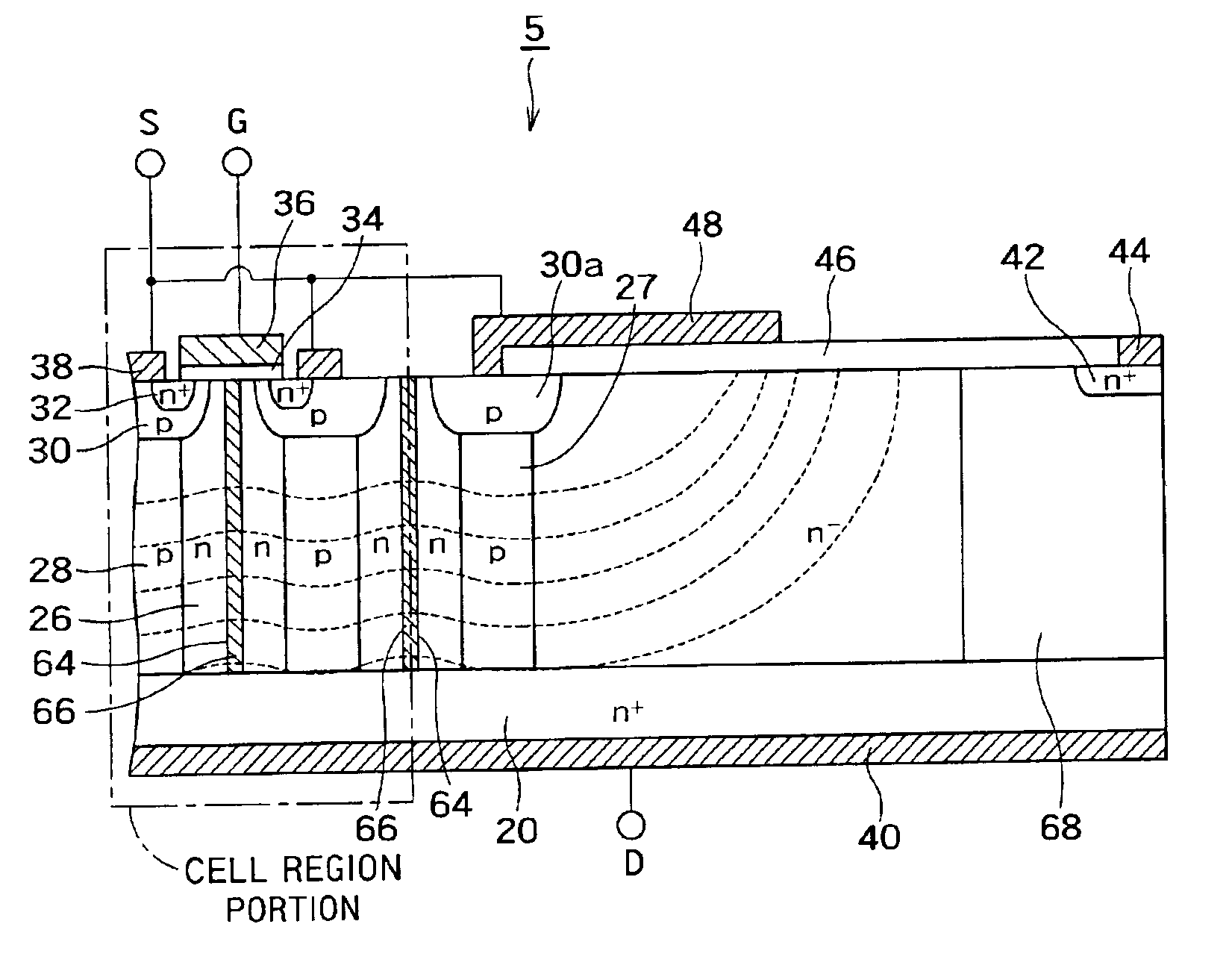
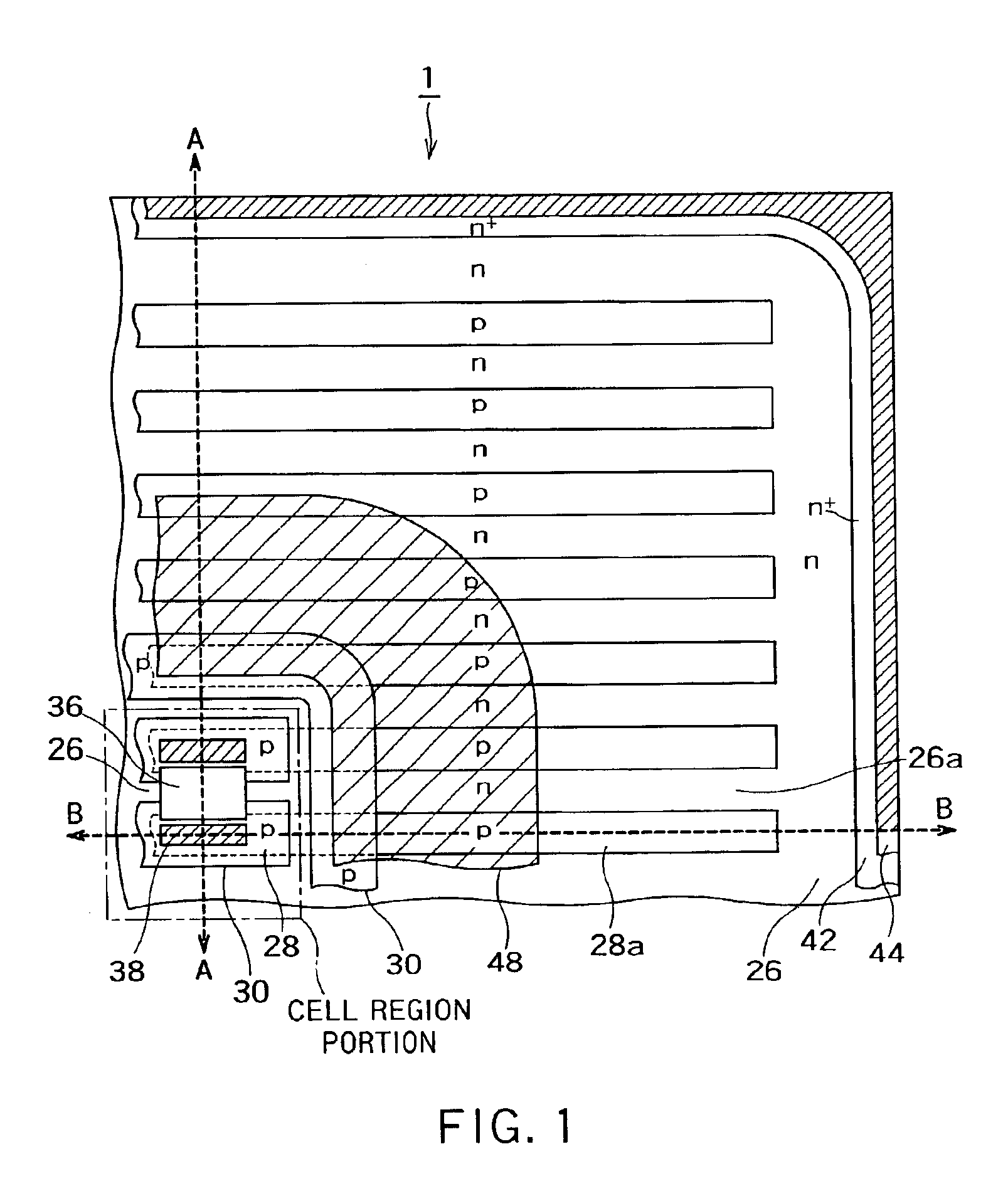
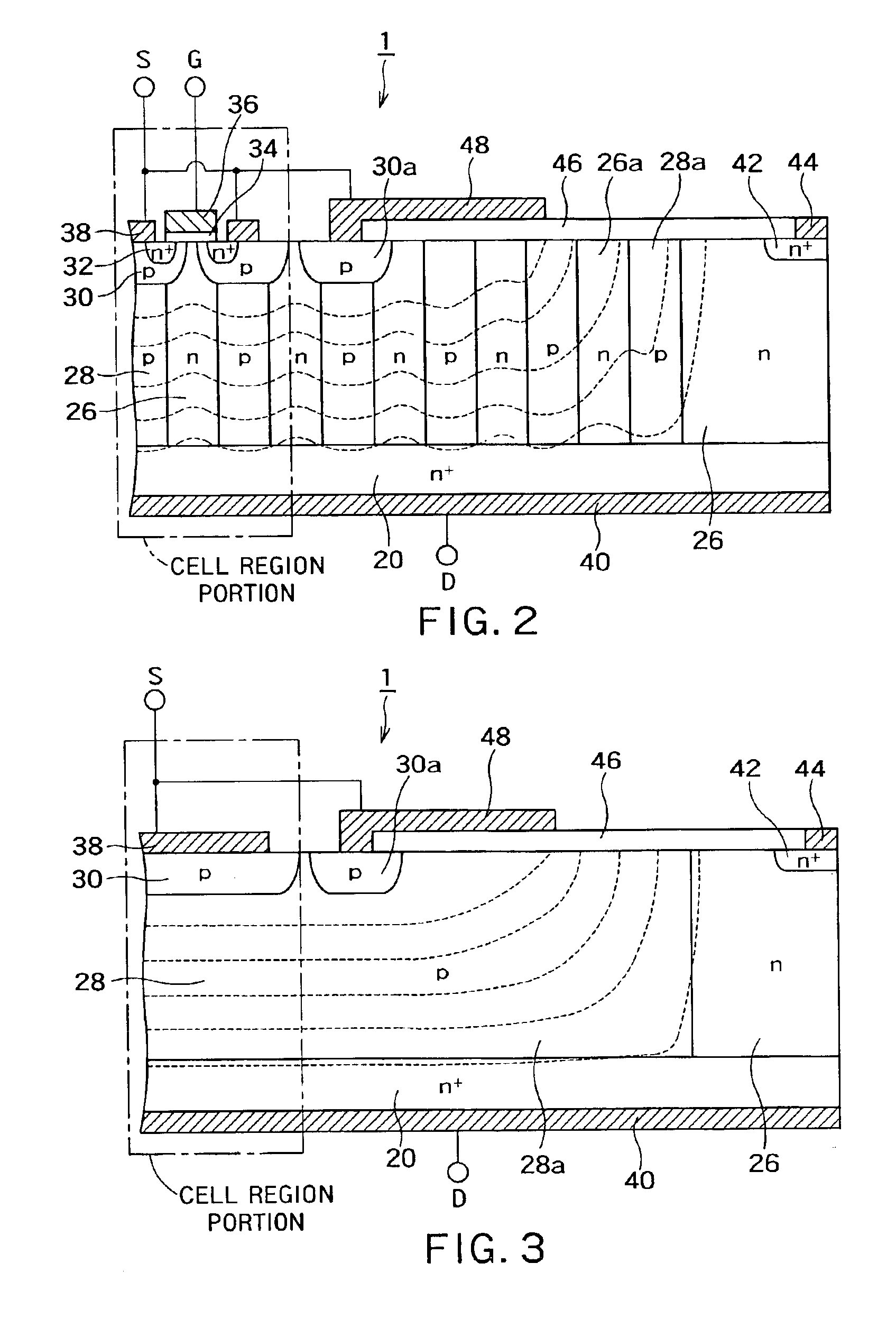
FIG. 1 is a plan view showing a schematic structure of a first embodiment of the semiconductor device according to the present invention. FIG. 2 and FIG. 3 are cross-sectional views of the semiconductor device of the present embodiment along taken along the cutting lines A—A and B—B of FIG. 1, respectively. As is clear in comparison with FIG. 36, the semiconductor device 1 of the present embodiment is characterized in that n− type drift layers 26 and p-type drift layers 28 are formed not only in a cell region portion, but are formed also up to the vicinity of the periphery of a junction terminating region portion. Hereinafter, the structure of the semiconductor device 1 of the present embodiment will be described in even more detail.

The semiconductor device 1 of the present embodiment has an n+ type drain layer 20, a drain electrode 40, the n type drift layers 26, the p type drift layers 28, p type base layers 30, an n+ type source layer 32, a source electrode 38...

second embodiment

(2) Second Embodiment

FIG. 4 is a plan view showing a schematic structure of a second embodiment of a semiconductor device according to the present invention. FIG. 5 and FIG. 6 are cross-sectional views of the semiconductor device of the present embodiment taken along the cutting lines A—A and B—B of FIG. 4, respectively.

The semiconductor device 2 of the present embodiment has, in place of the fieldplate electrode 48 which the semiconductor 1 shown in FIG. 1 has, a p− type resurf layer 52 which is connected to the p type base layer 30a disposed so as to surround the cell region in the junction terminating region portion, and which is formed so as to further surround the p type base layer 30a. The other structures of the semiconductor device 2 are substantially the same as those of the semiconductor device 1 shown in FIG. 1.

As shown by the equipotential lines in FIG. 2 and FIG. 3, also by providing such a p− type resurf layer 52, the electric field is attenuated at the time when the d...

third embodiment

(3) Third Embodiment

FIG. 7 is a plan view showing a schematic structure of a third embodiment of a semiconductor device according to the present invention. Note that a cross-sectional view taken along the cutting line A—A in the view is substantially the same as FIG. 2.

The semiconductor device 3 of the present embodiment is characterized in that p type drift layers 54, 54a have a circular plane shape, which is different from the above-described embodiments. Due to the p type drift layers being structured in such a shape, the depletion layers can be extended in all directions in a plane which is horizontal to the surface of the device.

Note that, in FIG. 7, although an example of circular patterns is shown, there may be polygonal patterns such as quadrangular patterns, hexagonal patterns, or the like. Further, it may be formed such that the n type drift layers 26 have a pattern. Further, in the same way as in the above-described second embodiment, a resurf layer can be applied in plac...


PUM


Abstract

A semiconductor device includes a first-conductivity-type semiconductor layer which includes a cell region portion and a junction terminating region portion. The junction terminating region portion is a region portion which is positioned in an outer periphery of the cell region portion to maintain a breakdown voltage by extending a depletion layer to attenuate an electric field.

Description

CROSS REFERENCE TO RELATED APPLICATIONThis application claims benefit of priority under 35USC § 119 to Japanese patent application No. 2002-74633, filed on Mar. 18, 2002, the contents of which are incorporated by reference herein.BACKGROUND OF THE INVENTION1. Field of the InventionThe present invention relates to a semiconductor device and a method of manufacturing a semiconductor device, and in particular, to a structure of a junction terminating region portion of a power semiconductor device which is suitable for a switching element for electric power.2. Related Background ArtIn response to the demand to make electrical power equipment compact and high-performance in recent years in the power electronics field, performance improvements with respect to making lowering loss, increasing speed and improving the ruggedness have been carried out in addition to making them have a high breakdown voltage and making them able to handle great current in the power semiconductor devices. Among...

Claims


Application Information

Patent Timeline
IPC IPC(8): H01L21/02H01L29/02H01L29/66H01L29/78H01L21/336H01L29/06H01L29/40
CPCH01L29/0634H01L29/0696H01L29/7811H01L29/66712H01L29/7802H01L29/402H01L29/0653H01L29/41741
Inventor YAMAGUCHI, MASAKAZUSAITO, WATARUOMURA, ICHIROIZUMISAWA, MASARU
Owner KK TOSHIBA
Why Eureka
Try Eureka