Method of fabricating waveguide channels

a technology of waveguide channels and manufacturing methods, applied in waveguide type devices, basic electric elements, electrical equipment, etc., can solve the problems of inability to manufacture such long channels, inability to use manufacturing such long channels, and high manufacturing costs

Inactive Publication Date: 2005-01-18
PETERSON STIG ANDERS
View PDF6 Cites 26 Cited by
  • Summary
  • Abstract
  • Description
  • Claims
  • Application Information

AI Technical Summary

Benefits of technology

The surface porosity can also be employed for manufacturing a structure attenuating electromagnetic waves, in particular microwaves. The a plate shaped body can be produced having cut-outs or recesses made in a first large surface of the body. Thereafter the first large surface is coated with electrically conducting material for forming an electrically conducting surface layer having a rough lower surface at the continuation to the permeable or non-attenuating material having a surface porosity. The interior surface of the conducting material obtains such a...

Problems solved by technology

This results in that the walls between the channels become long and narrow.
Manufacturing such long channels is impossible using the technology whi...

Method used


Image

  • Method of fabricating waveguide channels
  • Method of fabricating waveguide channels
  • Method of fabricating waveguide channels

Examples


Embodiment Construction

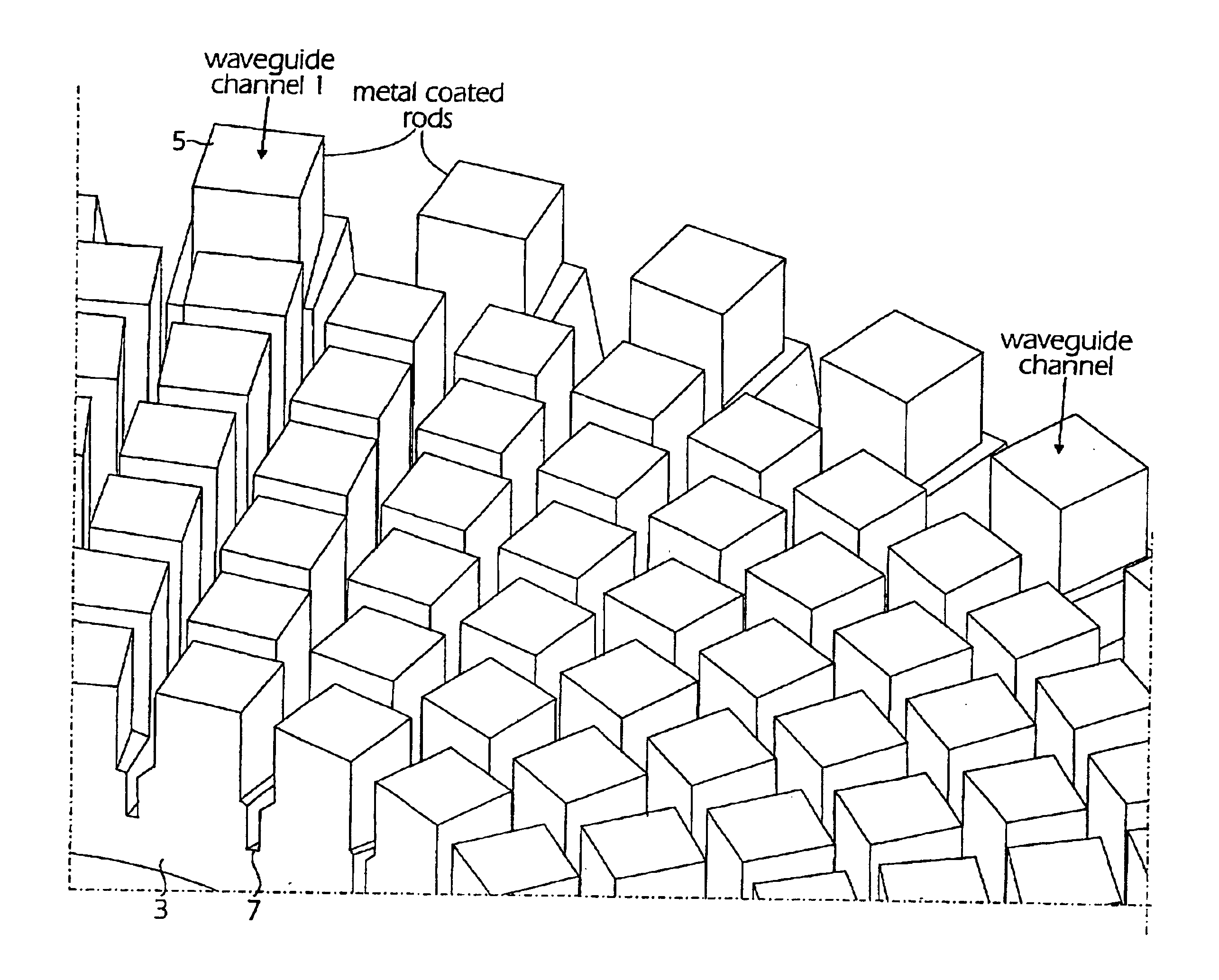
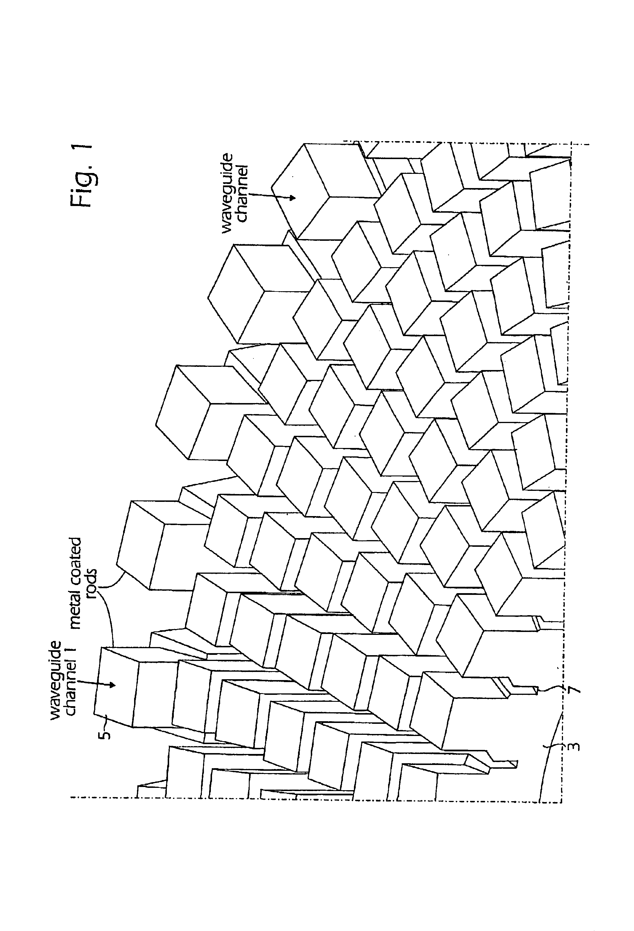
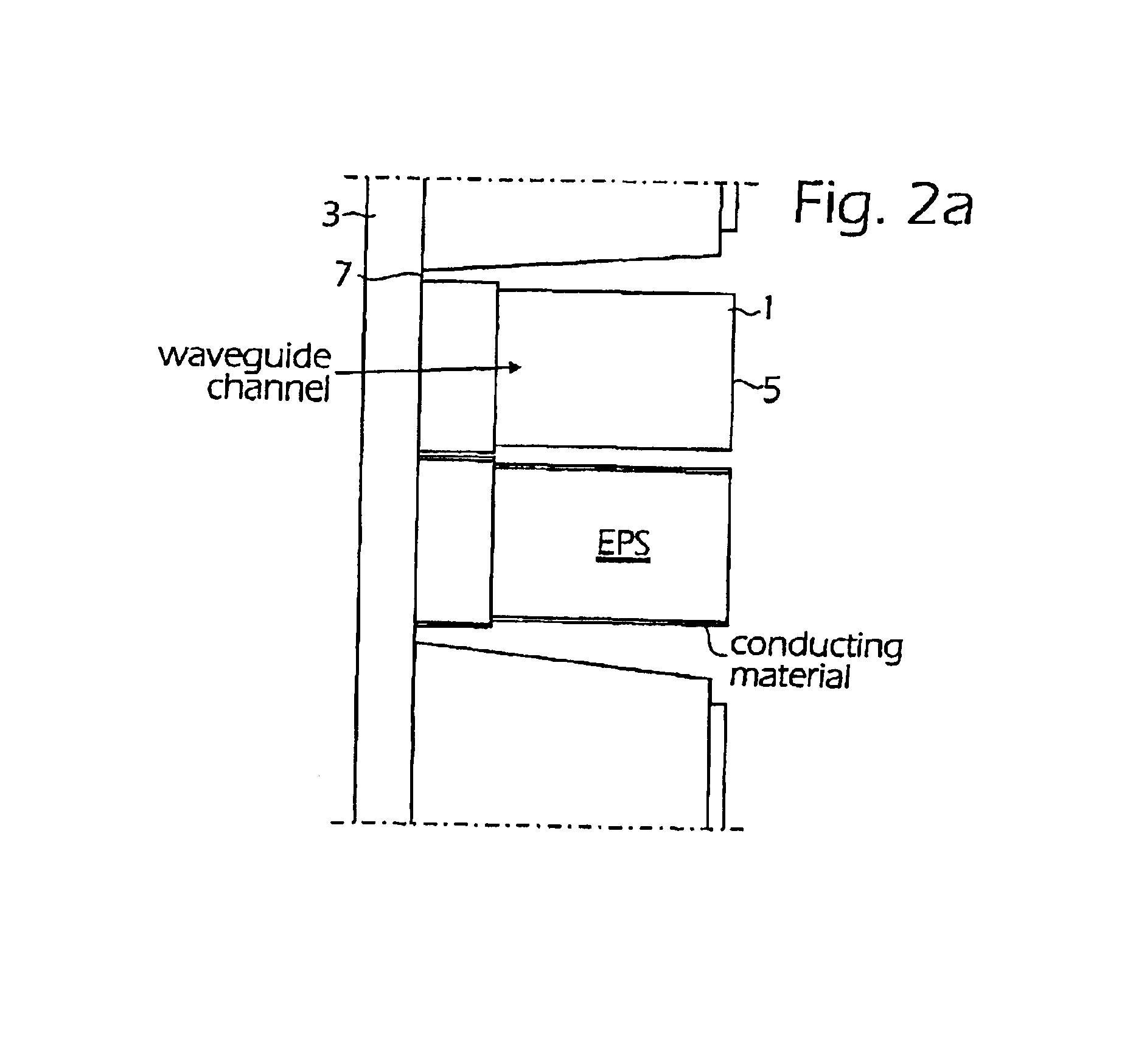
Materials exist which have such a low attenuation of electromagnetic waves that they can approximately be considered as air in spite of the fact that they in other respects have characteristics of solids. An example of such a material is EPS (Expanded PolyStyrene) that has an attenuation coefficient smaller than 0.1 dB / dm. This material can be easily used for manufacturing bodies having very varying shapes. In FIG. 1 is in a perspective view shown a portion of a waveguide antenna made from such a material having an insignificant attenuation for electromagnetic radiation, see also the part cross-sectional view of FIG. 2a. The waveguide antenna is formed from rods 1 that project to one side from a for example flat base plate 3 keeping the antenna together to form one unit. The rods 1 are on their side surfaces coated with an electrically conducting layer, see the description hereinafter. The end surfaces 5 of the rods have no such coating but in contrast there is a conducting coating ...


PUM

PropertyMeasurementUnit
Shapeaaaaaaaaaa
Electrical conductoraaaaaaaaaa
Dimensionaaaaaaaaaa

Abstract

When manufacturing waveguides, for example densely located waveguide channels, for electromagnetic waves such as microwaves, the channels are produced from rod-shaped bodies (1) of a material permeable to the waves and non significantly attenuating the waves. The bodies (1) can for example project from a base plate (3) and their side surfaces are coated with electrically conducting material but not their free end surfaces (5). The interior of the bodies form the waveguide channels, which have their walls formed from the layer of electrically conducting material. By giving the rod-shaped bodies suitable shapes for example an antenna side or half of a waveguide antenna can be manufactured. The rod-shaped bodies can before applying the electrically conducting material be coated with one or several layers of non-attenuating and non-conducting lacquer filling pores and smoothing the surface of the bodies. Thereby, the layer of electrically conducting material obtains a smooth transition surface to the material of the bodies giving the channels good waveguide characteristics. If the material used in the bodies has a strong surface porosity, the channels formed from the rod-shaped bodies become strongly attenuating to the electromagnetic waves. A set of such bodies located at the sides of each other and having suitable dimensions of the bodies gives an element working strongly attenuating to the electromagnetic waves.

Description

TECHNICAL FIELDThe present application relates to a method of manufacturing waveguide channels for microwaves, in particular waveguide channels arranged closely at or at the sides of each other, and furthermore a method of manufacturing elements for attenuating microwaves.BACKGROUNDIn waveguide antennas for receiving and transmitting electromagnetic radiation having frequencies in for example the GHz range the largest possible portion of the surface of the antennas should consist of open channels that are densely packed, i.e. are located closely at or at the sides of each other. This results in that the walls between the channels become long and narrow. Manufacturing such long channels is impossible using the technology which at present is available for mass production. Waveguide antennas having such channels are for example disclosed in the published International patent application WO 94 / 11920.Waveguide channels for microwaves are generally often made as metal tubes having accurat...

Claims


Application Information

Patent Timeline
IPC IPC(8): H01P11/00H01Q15/14H01Q3/26H01Q25/00H01Q15/04
CPCH01P11/002H01Q3/2658H01Q15/141H01Q25/007H01Q15/14Y10T29/49016
Inventor PETERSON, STIG ANDERS
Owner PETERSON STIG ANDERS
Why Eureka
Try Eureka