Modification of column fixed pattern column noise in solid state image sensors

Active Publication Date: 2005-01-18
STMICROELECTRONICS SRL
View PDF7 Cites 36 Cited by
  • Summary
  • Abstract
  • Description
  • Claims
  • Application Information

AI Technical Summary

Benefits of technology

The invention is preferably applicable to image sensors employing per-column ADC. Per-column ADC architectures have advantages of low power, low voltage operation. T

Problems solved by technology

The column elements add noise in the form of offset voltages to the pixel voltages.
This results in vertical shading of the output image, known as “column fixed pattern noise” (column

Method used


Image

  • Modification of column fixed pattern column noise in solid state image sensors
  • Modification of column fixed pattern column noise in solid state image sensors
  • Modification of column fixed pattern column noise in solid state image sensors

Examples


Example

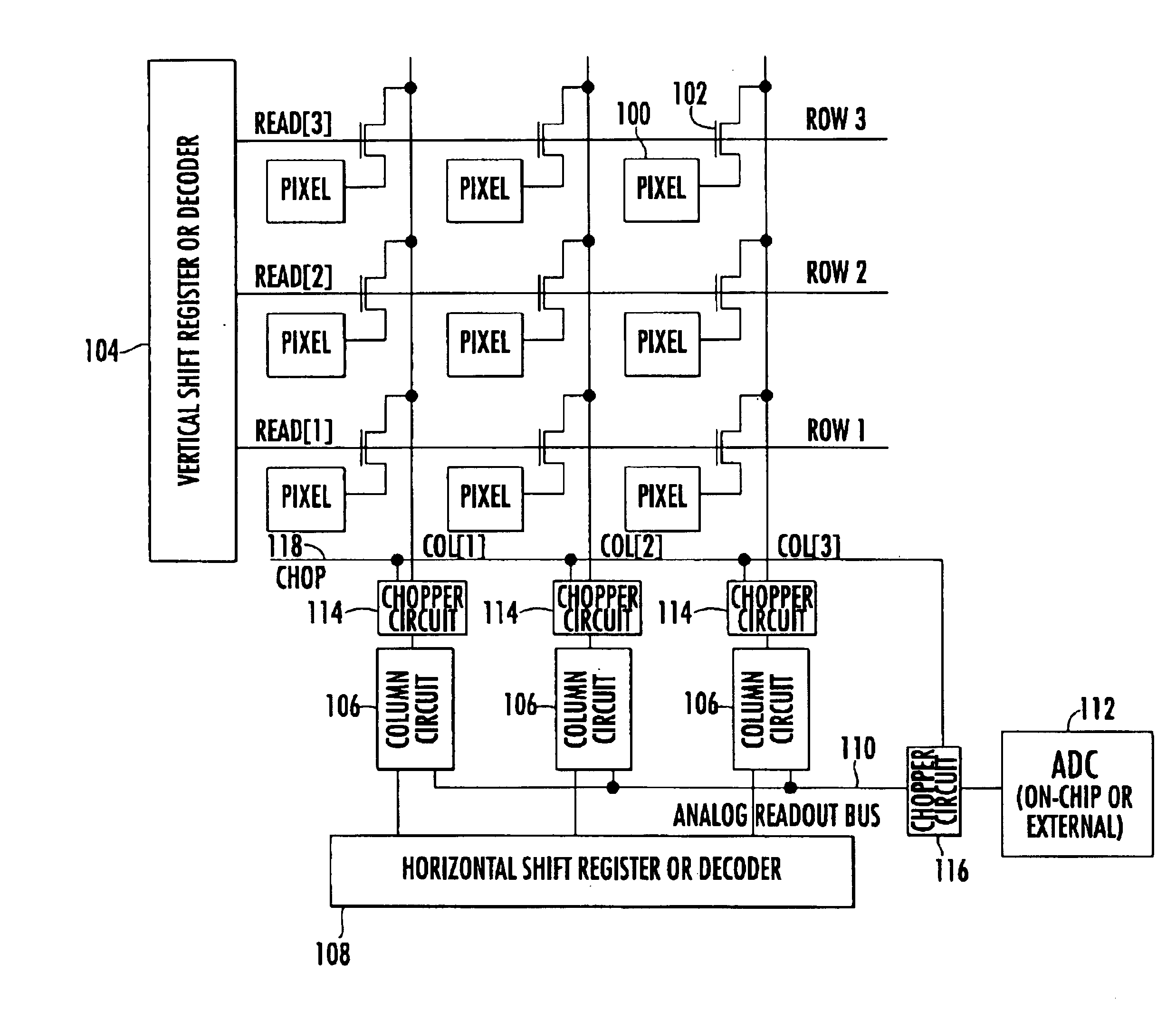
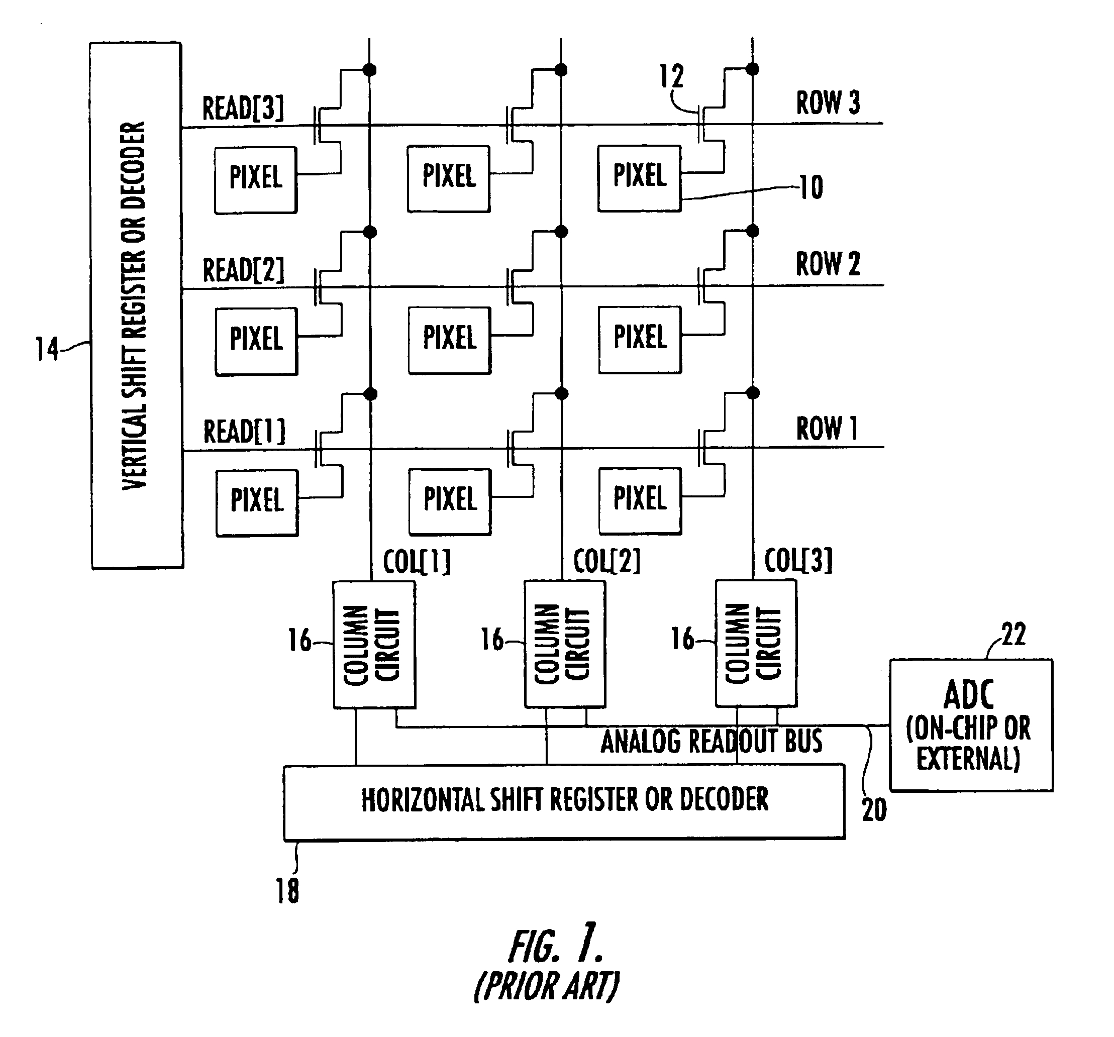
Referring now to the drawings, FIG. 3 shows an embodiment of a solid state image sensor with a per-chip ADC architecture, similar to that of FIG. 1, but modified to implement a column FPN reduction technique in accordance with the present invention. As in FIG. 1, the sensor comprises a matrix of pixels 100, associated read switches 102, a vertical shift register (decoder) 104, column element circuits 106, a horizontal shift register (decoder) 108, analog readout bus 110 and ADC 112. In addition, each column includes a first chopper circuit 114 upstream of the respective column element 106, and the readout bus 110 includes a second chopper circuit 116 downstream of the column elements 106 and prior to the ADC 112. The operation of the chopper circuits 114 and 116 is controlled by a common CHOP signal line 118.

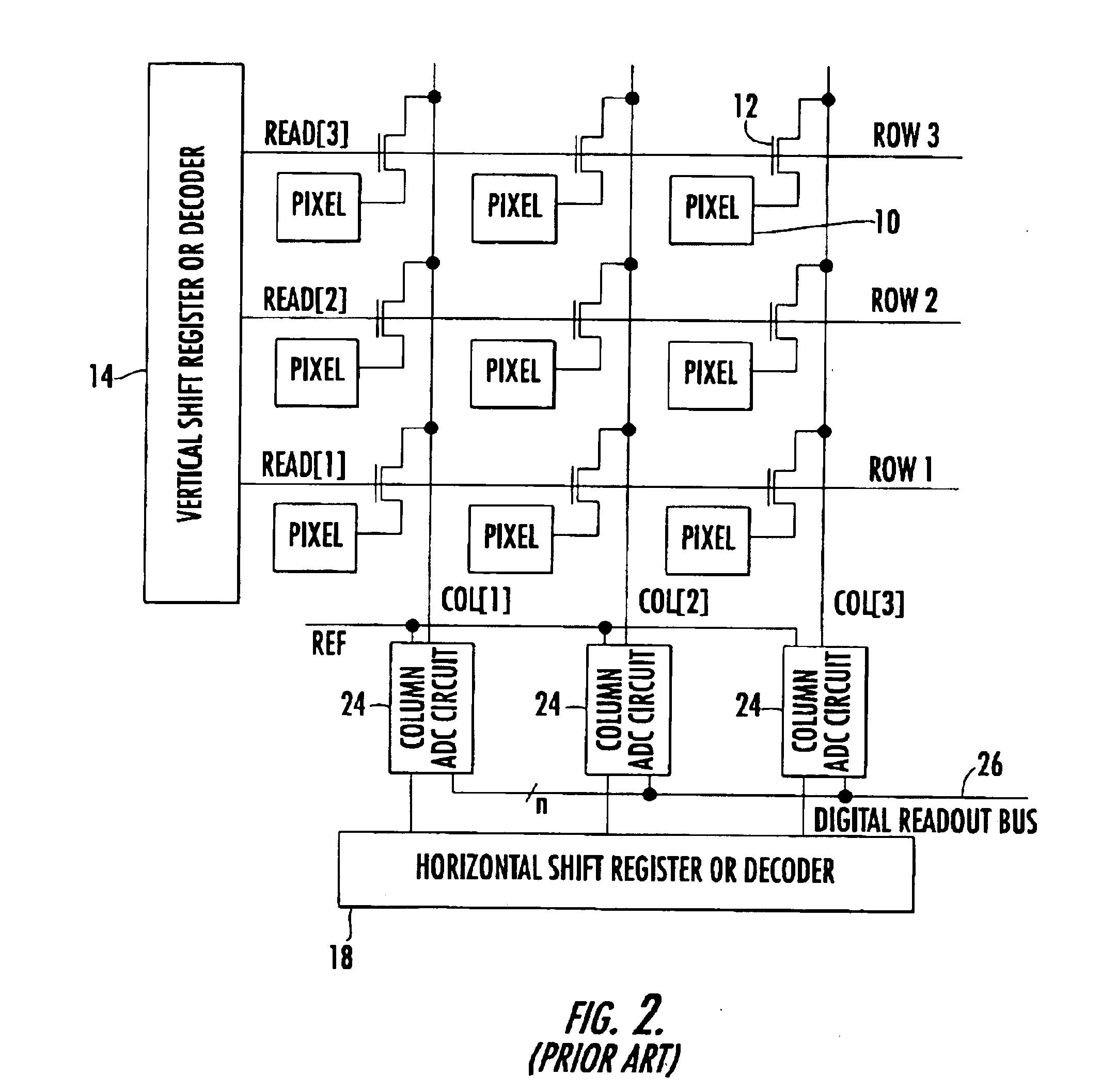
FIG. 4 shows a preferred embodiment of a solid state image sensor with a per-column ADC architecture, similar to that of FIG. 2, but again modified to implement a column FPN red...


PUM


Abstract

Solid state image sensors, and methods of operation thereof, includes an array of photosensitive pixels arranged in rows and columns and in which pixel data signals are read out from the pixels via column circuits, which introduces column fixed pattern noise to the signals. The signals are selectively inverted at the inputs to the column circuits and the inversion is reversed following output from the column circuits. Each column circuit may include an analog-to-digital converter and a digital inverter for inverting digital output therefrom. The selective inversion may be applied to alternate rows or groups of rows of the pixel data, and may be applied differently to different frames of the pixel data. These techniques result in column fixed pattern noise being modulated in a manner which makes the noise less apparent to the eye, and which facilitates subsequent cancellation of the noise.

Description

FIELD OF THE INVENTIONThe present invention relates to techniques for reducing the effects of column fixed pattern noise in solid state image sensors of the type comprising a matrix of photoelectric conversion elements. The techniques of the invention result in column fixed pattern noise being modulated in a manner which makes the noise less apparent to the eye and which facilitates subsequent cancellation of the noise.BACKGROUND OF THE INVENTIONIn an image sensor of this general type, the pixels are arranged in rows and columns and each pixel has a read switch which connects the pixel to a vertical line. Horizontal control lines activate the read switches of a row of pixels. These lines are pulsed in sequence to read the light dependent pixel voltages onto the vertical lines. A vertical shift register or decoder is commonly used to generate the read pulse sequence. The voltages on the vertical column lines then pass through a set of elements, one per column, which process the pixel...

Claims


Application Information

Patent Timeline
IPC IPC(8): H04N3/15H04N5/217H04N5/357H04N5/365H04N5/378
CPCH04N5/3575H04N5/378H04N5/3658H04N25/616H04N25/677H04N25/75
Inventor HENDERSON, ROBERTSMITH, STEWART GRESTYHURWITZ, JONATHAN EPHRIAM DAVID
Owner STMICROELECTRONICS SRL
Why Eureka
Try Eureka