Optical transistor and method thereof

a technology of optical transistors and transistors, applied in the field of optical switches, can solve the problems of slow switching time, easy to predict, and multiple sub-units connected together as a large complex system that cannot operate as a single unit, and achieve the effect of fast switching tim

Inactive Publication Date: 2005-01-25
II VI DELAWARE INC
View PDF9 Cites 7 Cited by
  • Summary
  • Abstract
  • Description
  • Claims
  • Application Information

AI Technical Summary

Benefits of technology

[0011]The present invention discloses an optical transistor that provides a fast switching time, an amplified gain, and unidirectional signal flow isolation. The optical transistor receives a small optical input signal at an optical base port, generates an amplified replica at an optical emitter port, and generates a phase inverted replica at an optical collector port. One embodiment of the optical transistor is implemented with a vert...

Problems solved by technology

Even though each sub-unit behaves as a single unit, multiple sub-units connected together as a large complex system do not operate as a single, easily predictable unit.
The bi-directionality of a large complex system hinders the ability to predict the performance based on single unit characteristics.
Prior research and development in the design of an optical transistor have resulted in...

Method used


Image

  • Optical transistor and method thereof
  • Optical transistor and method thereof
  • Optical transistor and method thereof

Examples


Embodiment Construction

low chart illustrating the functional process for operating an optical transistor in accordance with the present invention.

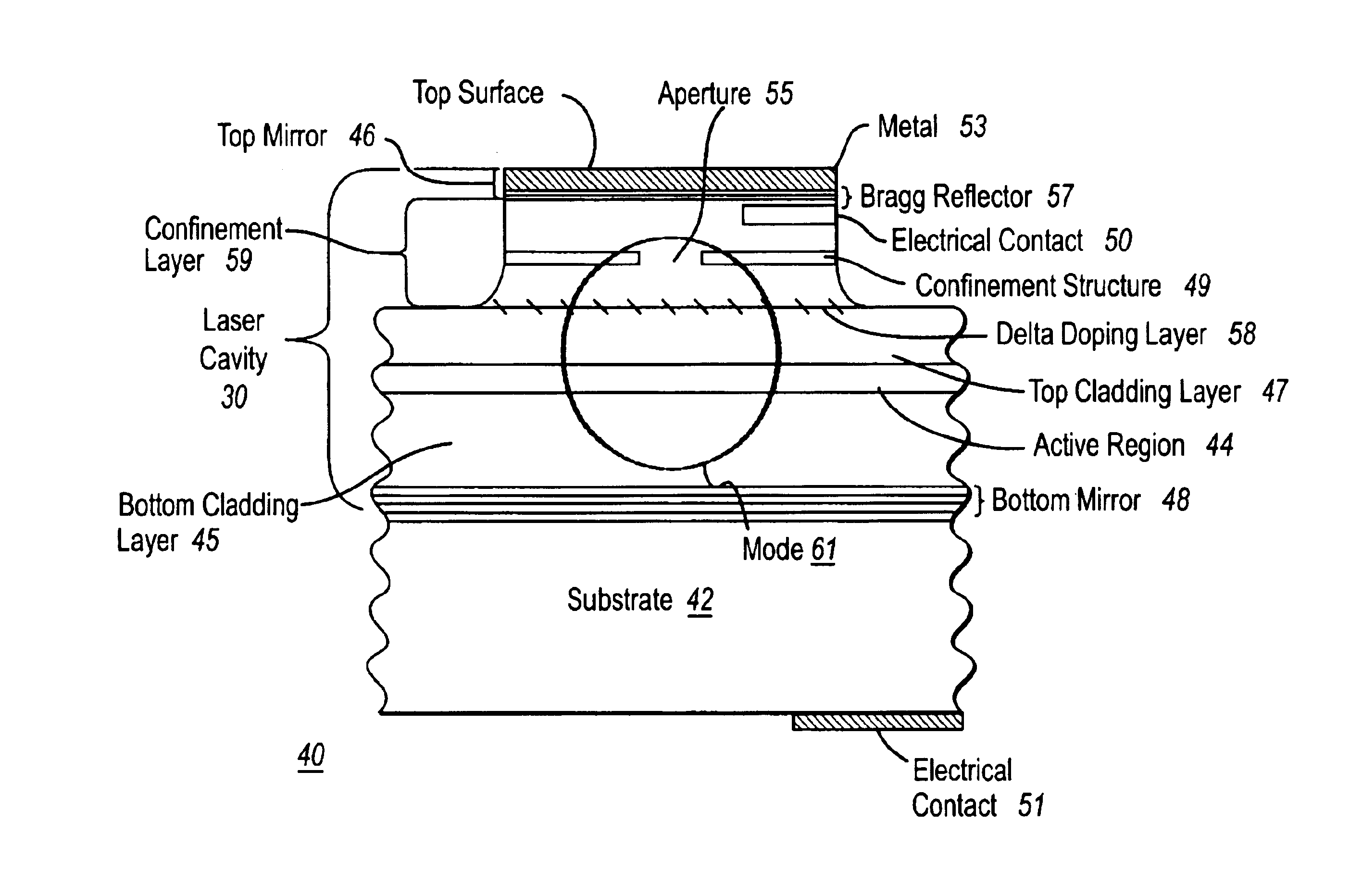
[0018]FIGS. 4A-4C are a perspective view, transverse cross-section, and longitudinal cross-section, respectively, of one embodiment of a vertical lasing semiconductor optical amplifier (VLSOA) in according to the present invention.

DETAILED DESCRIPTION OF THE PREFERRED EMBODIMENT(S)

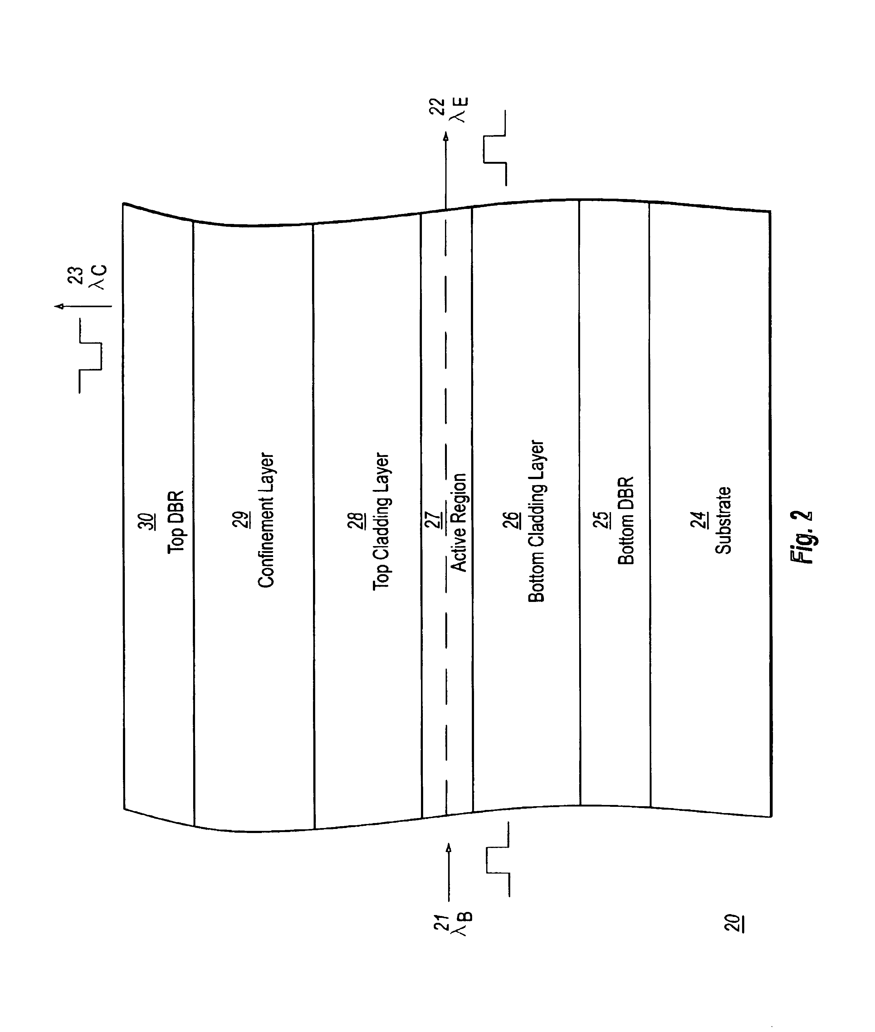
[0019]An apparatus and method for designing an optical transistor is described. In the following description, for purposes of explanation, numerous specific details are set forth in order to provide a thorough understanding of the present invention. It will be evident, however, to one skilled in the art that the present invention may be practiced without these specific details. For example, a parallel analogy can be drawn between an electrical transistor and an optical transistor. Consequently, all circuits using electrical-based transistors that are biased in the forward active mode c...


PUM


Abstract

An optical transistor is disclosed that provides a fast switching time, an amplified gain, and isolation. The optical transistor receives a small optical input signal at an optical base port, generates an amplified replica at an optical emitter port, and generates an inverted replica on a vertical light at an collector port. One embodiment of the optical transistor is implemented with a vertical lasing semiconductor optical amplifiers (VLSOA), wherein the ballast light is used a signal for the collector port.

Description

BACKGROUND INFORMATION[0002]1. Field of the Invention[0003]The present invention relates generally to the field of optics, and more particularly to optical switches.[0004]2. Description of Related Art[0005]A transistor in the traditional sense has three electrical contacts for use as a switch, amplifier, or detector. The recent explosion in optical technologies for transferring information at light speed is resulting in a shift from electrical-centric networks to all-optical networks. Conventional wisdom dictates that the use of electrical transistors for switching in a system design is due to the historical belief that electrons and holes are more suitable to attain faster switching times than photons.[0006]FIG. 1 is a prior art circuit diagram illustrating a Bipolar Junction Transistor (BJT) transistor 10. The electrical transistor 10 is constructed with three terminals, a base B 11a, an emitter E 12a, and a collector C 13a. The base B 11a serves as an input, while the emitter E 1...

Claims


Application Information

Patent Timeline
IPC IPC(8): H01L29/02H01L29/16
CPCG02F2/004G02F3/026H01S5/0608H01S5/5072H01S5/18311H01S5/2009H01S5/1032
Inventor DIJAILI, SOL P.WALKER, JEFFREY D.
Owner II VI DELAWARE INC
Why Eureka
Try Eureka