Pixel driving circuit system and method for electroluminescent display

a technology of electroluminescent display and driving circuit, which is applied in the field of illumination displays, can solve the problems of reducing the emission luminance of the oled, affecting the correct gradation display, and uneven display over the entire organic el display, and achieves the effect of reducing the kickback voltag

Inactive Publication Date: 2005-01-25
INNOLUX CORP
View PDF4 Cites 26 Cited by
  • Summary
  • Abstract
  • Description
  • Claims
  • Application Information

AI Technical Summary

Benefits of technology

Therefore, an object of the present invention is to effectuate correct gradation display on an OLED display device by reducing a kickback voltage attributable to parasitic capacitance of a switching TFT.

Problems solved by technology

For this reason, the decrease in the gate voltage of the driving TFT attributable to the kickback voltage greatly decreases the emission luminance of the OLED, whereby correct gradation display is impeded.
Moreover, display unevenness occurs over the entire organic EL display.
That is undesirable, as it leads to a decrease in the emission-contributable area of the OLED pixel circuit instead.
However, the OLED (the organic EL) deteriorates faster under increased current density, thus shortening its lifetime.
Therefore, increasing the electric current is not desirable.

Method used


Image

  • Pixel driving circuit system and method for electroluminescent display
  • Pixel driving circuit system and method for electroluminescent display
  • Pixel driving circuit system and method for electroluminescent display

Examples


Embodiment Construction

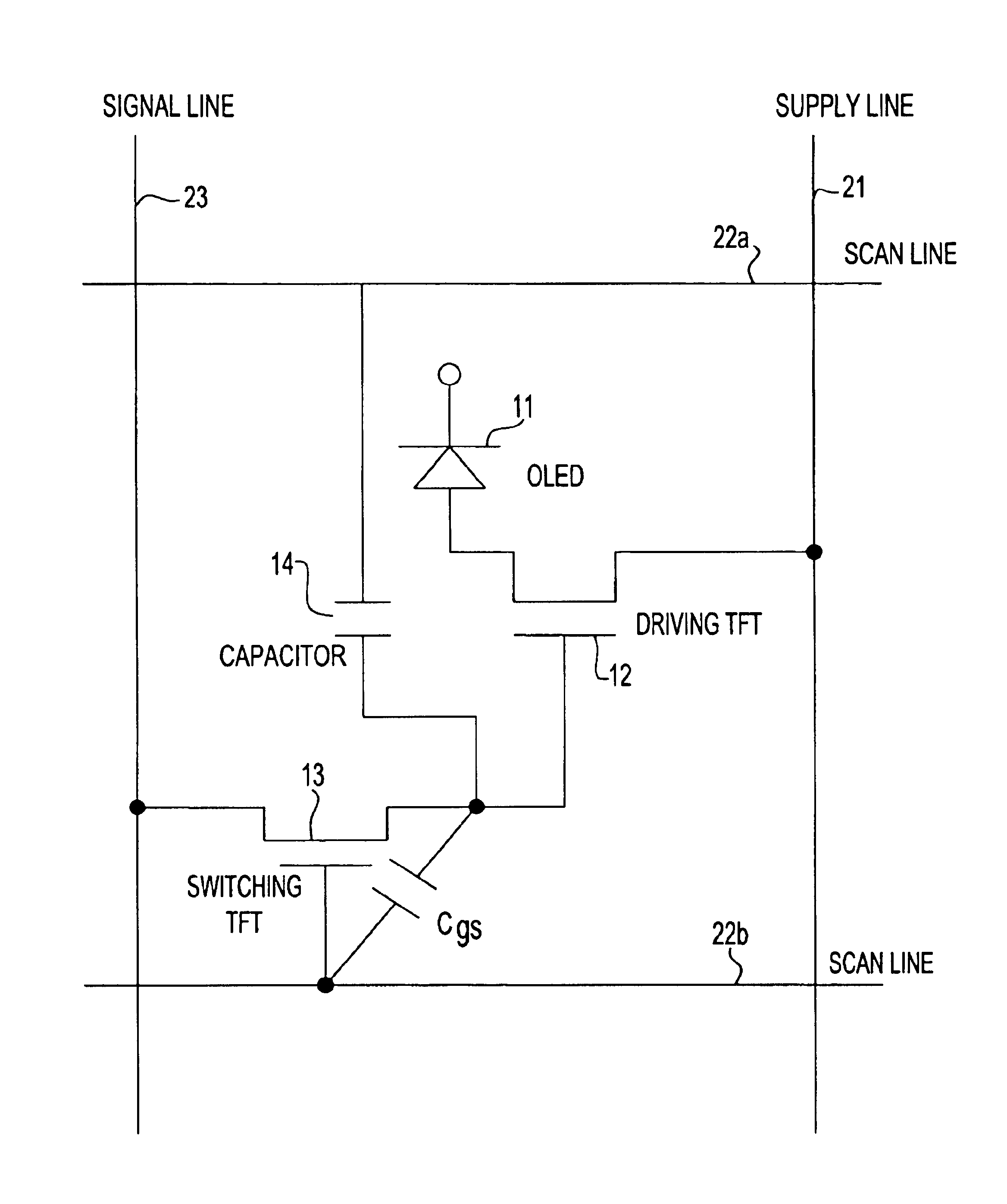
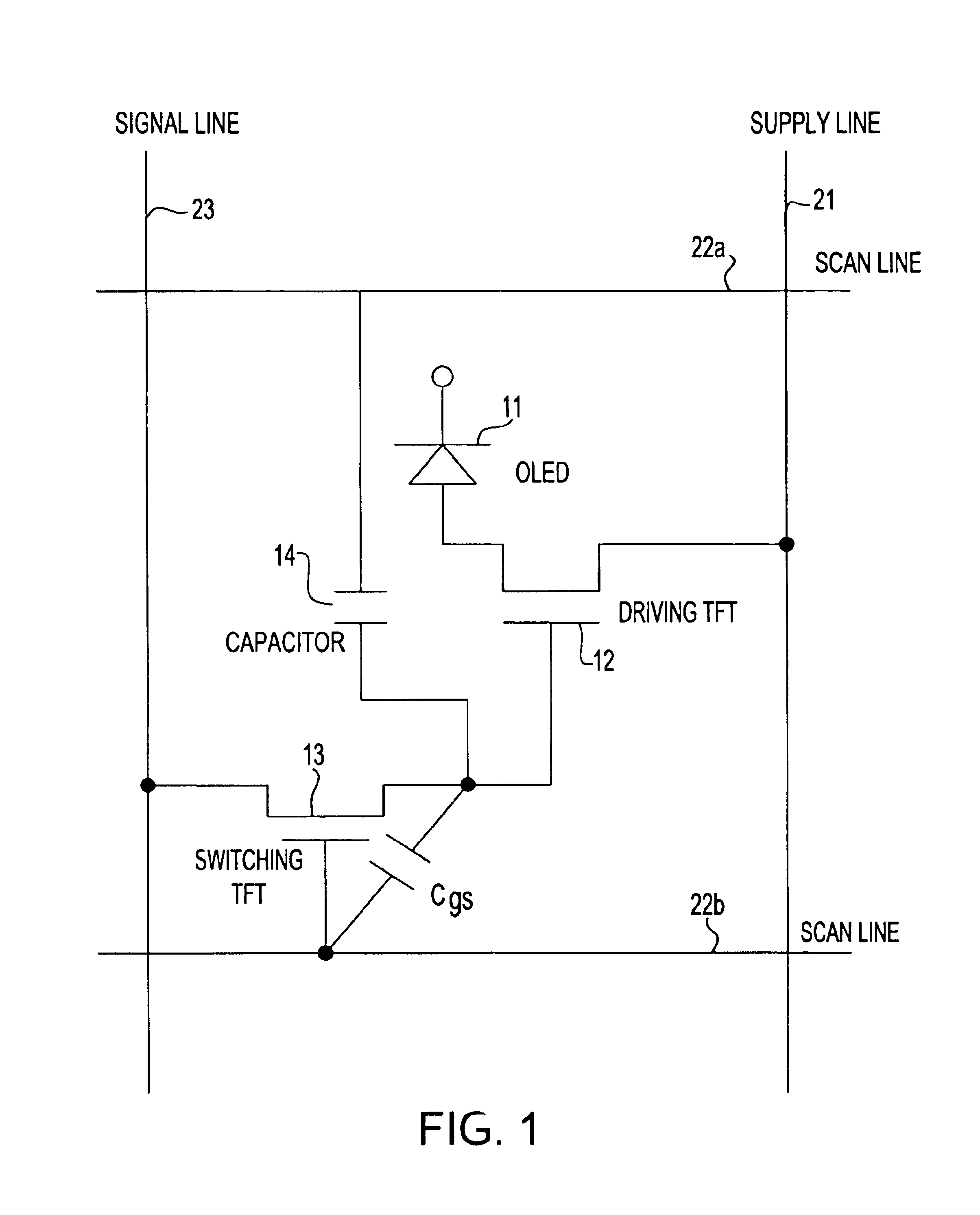
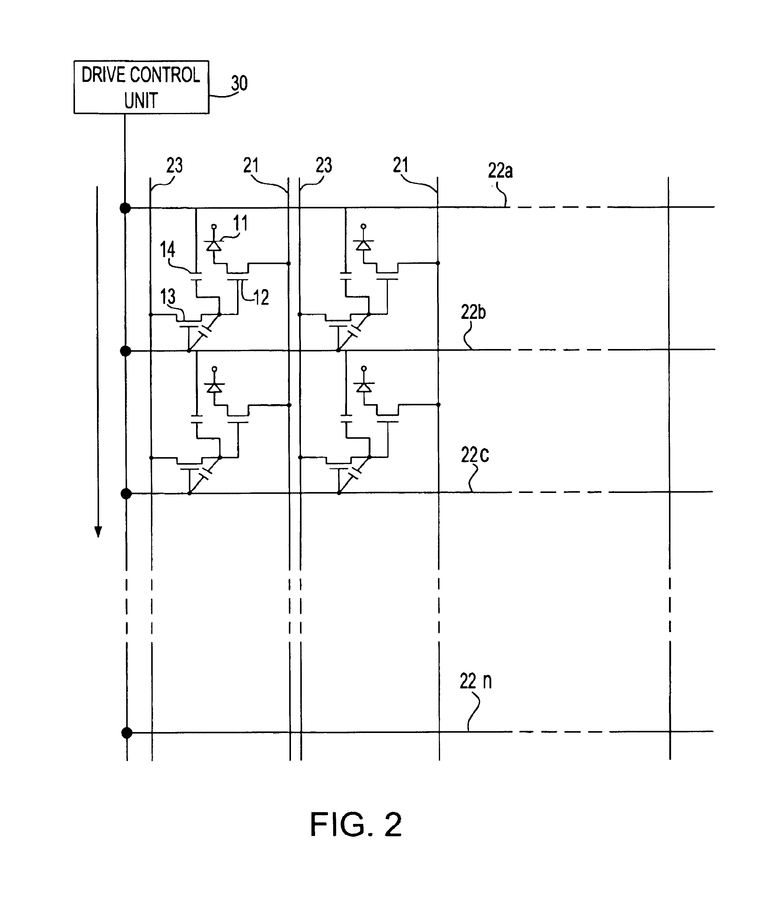
Embodiments of the invention will now be described with reference to the accompanying drawings. FIG. 1 is a diagram illustrating an OLED pixel circuit according to an embodiment. With reference to FIG. 1, the OLED pixel circuit of the embodiment includes an OLED 11 which is a light emitting element, a driving TFT 12 coupled to drive the OLED 11, a switching TFT 13 and a capacitor 14, those being disposed in a space surrounded by a supply line 21, scan lines 22 and a signal line 23 in gridiron. Moreover, a display panel for an organic EL display is made of a pixel array in which OLED pixel circuits of FIG. 1 are arranged in a matrix, as shown schematically in FIG. 2.

In FIG. 2, a drive control unit 30 includes scan pulse generating means for generating a scan pulse which instructs imaging timing to display an image on the display panel, and outputting means to output the scan pulse to each scan line 22a, 22b, 22c, etc. to supply the scan pulse to each of the OLED pixel circuits. In th...


PUM


Abstract

Accurate gradation display on an OLED display device is effectuated by reducing a kickback voltage based on parasitic capacitance of a switching TFT without increasing a capacitance of a capacitor which retains a voltage to be supplied to a driving TFT. A capacitor for maintaining on-and-off states of a driving TFT which drives an OLED is charged by a switching TFT. The capacitor is connected to a scan line, which drives a switching TFT located in a preceding stage in accordance with a scanning order. After being charged by the switching TFT, a reference potential on the capacitor is raised to compensate for a drop in a gate voltage of the driving TFT attributable to parasitic capacitance of the switching TFT, in accordance with a signal from the scan line.

Description

FIELD OF THE INVENTIONThe present invention relates to illuminated displays, a more specifically to a system and method for driving an organic light emitting diode pixel circuit in an organic electroluminescent display device.BACKGROUND OF THE INVENTIONAn organic electroluminescent (EL) display is a flat panel display for use as a computer or television monitor. A preferred method of driving an organic EL display is by an active matrix driving method, which provides a high-quality display image, while eliminating crosstalk. In an active matrix driving method, a thin-film transistor (TFT) is generally used as a switching element for an organic light emitting diode (OLED). OLED's are EL elements which operate by organic electroluminescence (EL).FIG. 7 is a view showing a general constitution of an OLED pixel circuit driven by a TFT. With reference to FIG. 7, a conventional OLED pixel circuit includes an OLED 711 which is a light-emitting element, a driving TFT 712 for driving the OLED...

Claims


Application Information

Patent Timeline
Patent Type & Authority Patents(United States)
IPC IPC(8): G09G3/32H01L51/50G09G3/20G09G3/30
CPCG09G3/3233G09G2300/0465G09G2300/0852G09G2300/0861G09G2320/0233G09G2320/0209G09G2320/0219G09G2320/0223G09G2300/0866
Inventor SUZUKI, HIROSHI
Owner INNOLUX CORP
Why Eureka
Try Eureka