Optical waveguide type microplate

a microplate and optical waveguide technology, applied in the field of optical waveguide type microplates, can solve the problems of reducing detection accuracy, difficult to accurately measure absorbance, and high cost of the elisa method described abov

Inactive Publication Date: 2005-01-25
KK TOSHIBA
View PDF4 Cites 31 Cited by
  • Summary
  • Abstract
  • Description
  • Claims
  • Application Information

AI Technical Summary

Problems solved by technology

The reagent used in the ELISA method described above is expensive.
This makes accurate absorbance measurement difficult, leading to a decrease in the detection accuracy.

Method used


Image

  • Optical waveguide type microplate
  • Optical waveguide type microplate
  • Optical waveguide type microplate

Examples


Embodiment Construction

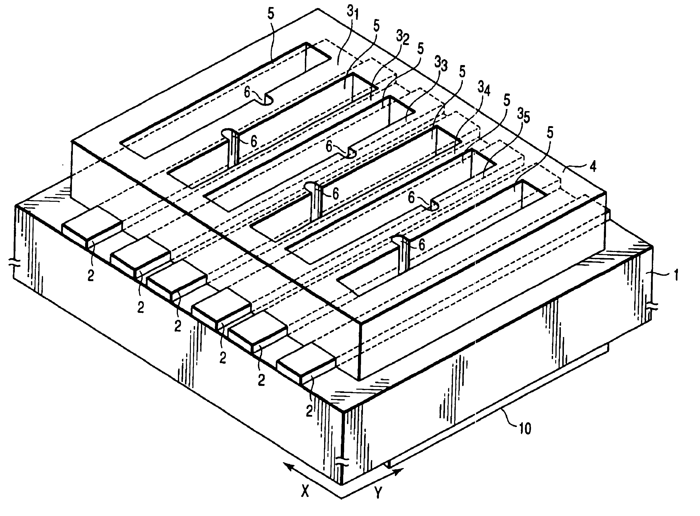
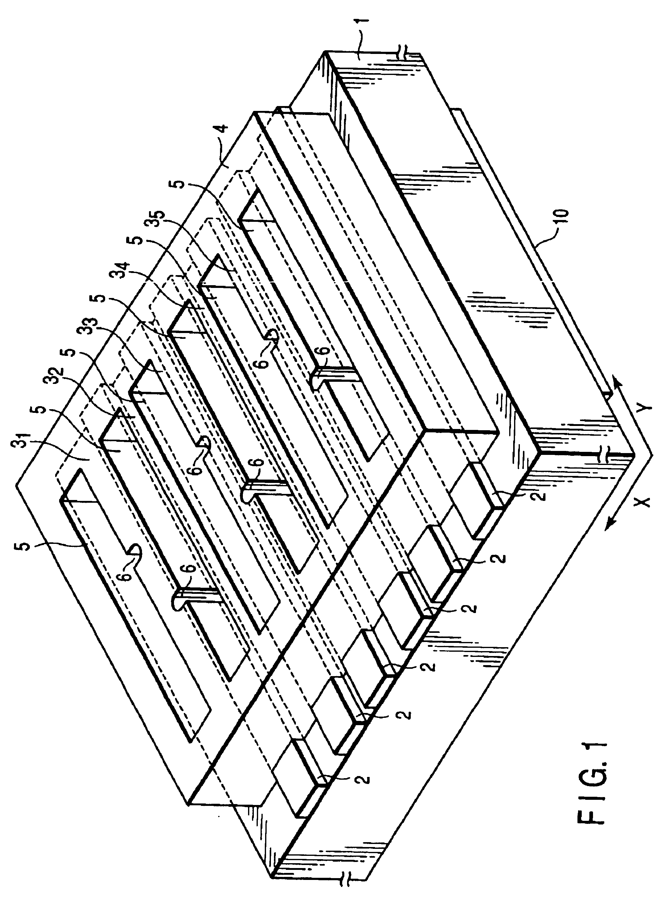
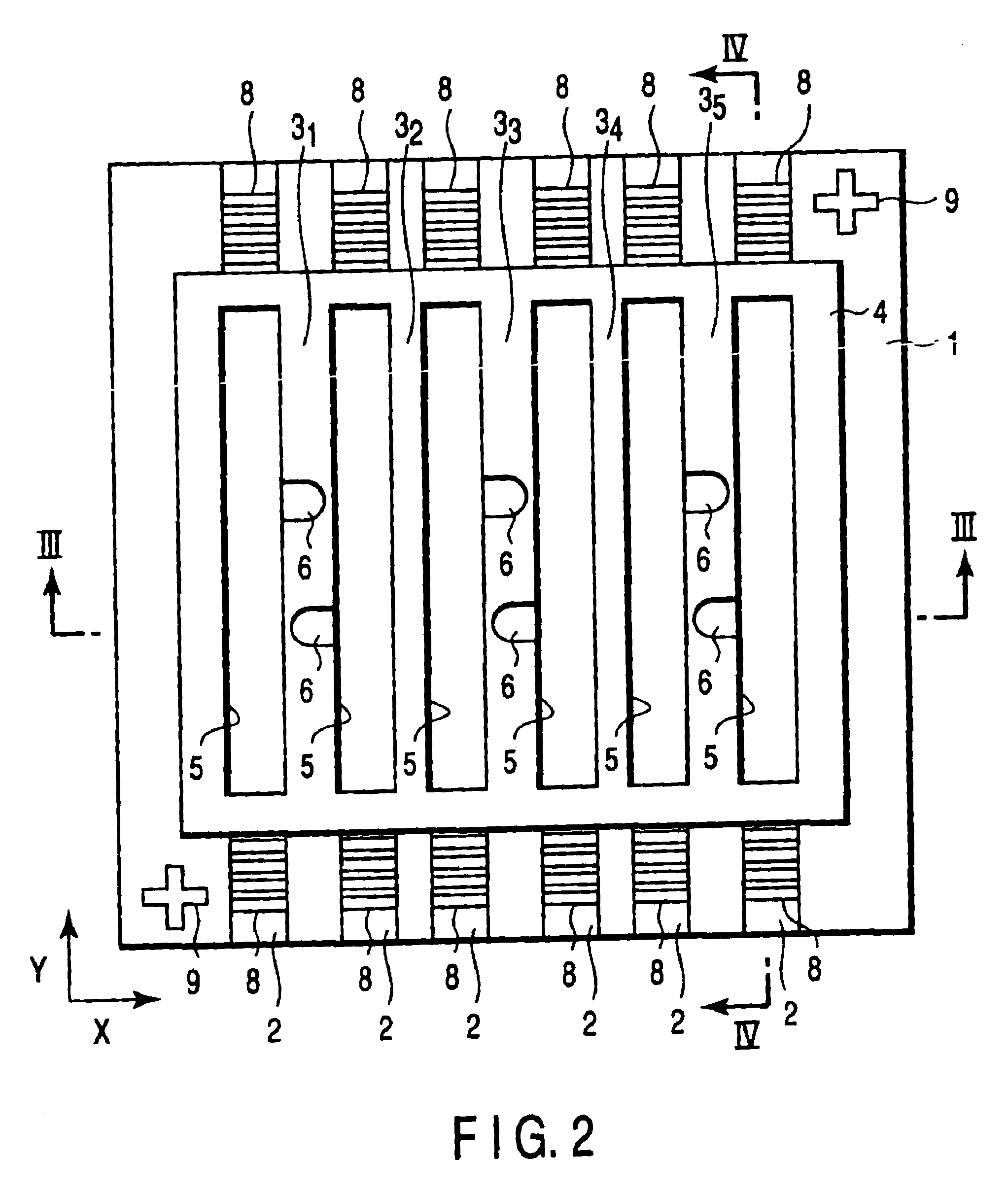
An optical waveguide type microplate of the present invention will be described in detail below with reference to the accompanying drawing.

FIG. 1 is a perspective view (gratings and alignment marks are not shown) showing an optical waveguide type microplate according to an embodiment of the present invention. FIG. 2 is a plan view of FIG. 1. FIG. 3 is a sectional view taken along a line III—III in FIG. 2. FIG. 4 is a sectional view taken along a line IV—IV in FIG. 2.

As shown in FIGS. 1 and 2, on one surface of a substrate 1 made of glass such as borosilicate glass, six band-like optical waveguide layers 2 extend in the Y-axis direction. These optical waveguide layers 2 have a refractive index higher than that of the substrate 1. Each optical waveguide layer 2 is formed by ion exchange of an element such as potassium or sodium with the glass component of the glass substrate 1.

The material of the substrate 1 is not limited to borosilicate glass. That is, it is also possible to use sil...


PUM

PropertyMeasurementUnit
refractive indexaaaaaaaaaa
heightaaaaaaaaaa

Abstract

An optical waveguide type microplate includes a substrate, a well formed on one surface of the substrate to receive a solution to be tested, an optical waveguide layer formed on a portion or the whole of a surface of the well contacted with the solution, a light incident member formed on the surface near one end portion in the longitudinal direction of the optical waveguide layer, and a light exist member formed on the surface near other end portion in the longitudinal direction of the optical waveguide layer.

Description

CROSS-REFERENCE TO RELATED APPLICATIONSThis application is based upon and claims the benefit of priority from the prior Japanese Patent Application No. 2002-40418, filed Feb. 18, 2002, the entire contents of which are incorporated herein by reference.BACKGROUND OF THE INVENTION1. Field of the InventionThe present invention relates to an optical waveguide type microplate for use in biochemical testing, clinical testing, and the like.2. Description of the Related ArtFor example, an enzyme-linked immuno adsorbent assay method (ELISA method) adopted in clinical testing uses a microplate made of a glass or synthetic resin substrate on the surface of which a plurality of wells are formed. That is, an antibody is immobilized on the well inner surface of this microplate, and a solution to be tested containing an antigen is placed in this well to cause an antigen antibody reaction. Subsequently, an enzyme-labeled antibody is placed in the well and labeled by combining the antibody with the a...

Claims


Application Information

Patent Timeline
Patent Type & Authority Patents(United States)
IPC IPC(8): B01L3/00G01N21/03G01N21/25G02B6/124G02B6/42G01N21/64G01N21/27G01N33/543G02B6/12
CPCB01L3/5085G01N21/253G02B6/124G01N21/0303B01L2300/0654B01L2300/0819G02B6/4214
Inventor UCHIYAMA, KENICHI
Owner KK TOSHIBA
Why Eureka
Try Eureka