Micro-controller protected against current attacks

Inactive Publication Date: 2005-02-01
GEMPLU
21 Cites 21 Cited by

AI-Extracted Technical Summary

Problems solved by technology

Given that the energy consumption of the said efficient data processing part may be considered as being directly proportional to the square of ...

Abstract

The invention concerns a microcontroller (30) intended to be incorporated in a portable object (1) of type smartcard, including at least:
    • a contact stud (VCC) to supply the said microcontroller (30) with current; a data input and/or output contact stud (I/O); an efficient data processing part (μCE); and confidential information. According to the invention, the microcontroller also includes: means (GEN, CAP, COM) to vary the supply voltage of the efficient data processing part (μCE), the said means being able to secure the said confidential data against current attacks.

Application Domain

Digital data processing detailsSemiconductor/solid-state device details +13

Technology Topic

VoltageEngineering +5

Image

  • Micro-controller protected against current attacks
  • Micro-controller protected against current attacks
  • Micro-controller protected against current attacks

Examples

  • Experimental program(1)

Example

The portable objects according to the invention are standardised objects defined in particular in the various section of standard ISO7816 whose content is incorporated in this description by giving the reference. In the mode of realisation shown on FIGS. 1, 2 and 3, such an object takes the form of a roughly rectangular thin card 1 including a body 2 integrated to an electronic module 3.
The body 2 of the card consists, for example, of five plastic laminated sheets 20, 21, 22, 23 and 24 and includes a cavity 25 to incorporate the module 3.
Module 3 includes a microcontroller 30 whose contact studs 300 are electrically connected, via conducting wires 31, to contact pads 32 flush with the surface of the card body 2. These contact pads 32 rest on a thickness 33 of an epoxy glass type dielectric. The assembly microcontroller 30 and conducting wires 31 is coated with a protective resin 34.
DETAILED DESCRIPTION
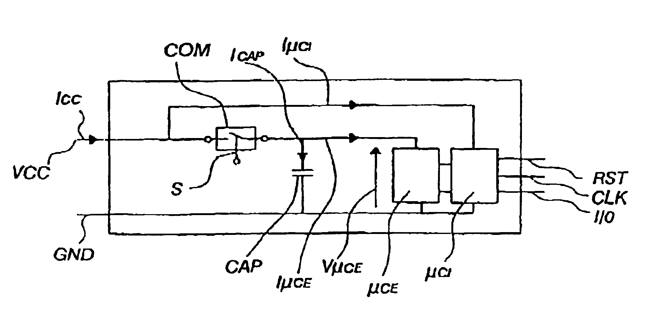
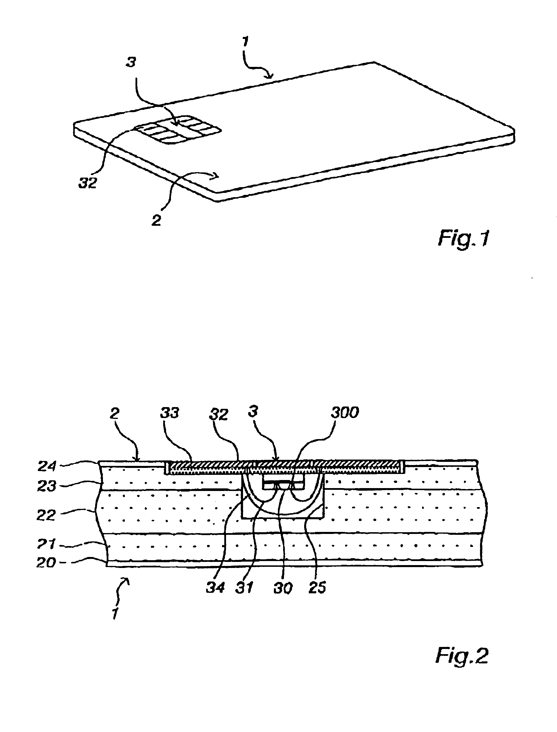
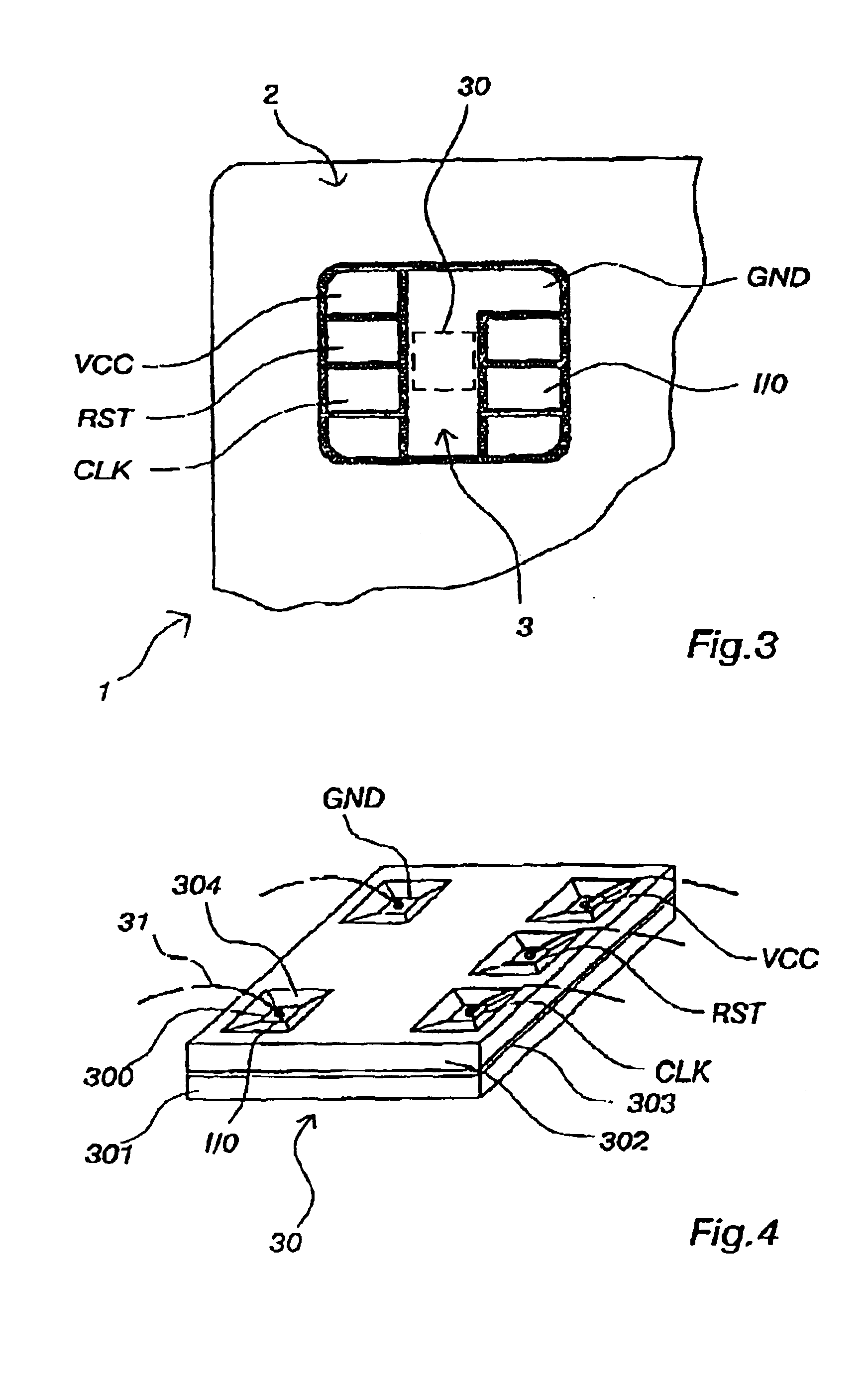
In the mode of realisation shown on FIG. 4, the microcontroller 30 takes the form of a right parallelepiped of thickness about 180 μm and area about 10 mm2.
This microcontroller 30 includes a main layer 301 of silicon whose active face, which includes a circuit and supports the contact studs 300, is sealed to an additional protective layer 302 of silicon using a sealing layer 303. This additional layer 302 has openings 304 located opposite the contact studs 300 so that they can be connected to the contact pads 32.
In practice, there are five contact studs 300. They are the studs VCC, RST, CLK, I/O and GND respectively connected to the contact pads VCC, RST, CLK, I/O and GND of module 3. The supply contact stud VCC is intended to power the microcontroller. The reset stud RST is intended to transmit a reset signal to the microcontroller, the clock stud CLK is intended to transmit a clock signal to the microcontroller, the input/output stud I/O is intended to enable the exchange of logical data between the microcontroller and the outside world, and the ground stud GND is used to connect the microcontroller to ground.
The integrated circuit of the microcontroller 30 according to the invention includes several active parts. In particular, there is an interface microcontroller part μCI and an efficient data processing part μCE shown on FIG. 5.
The interface microcontroller part or interface microcontroller μCI preferably only includes means which consume energy that is not likely to reveal information concerning the confidential data processed by the microcontroller. In practice, the interface microcontroller μCI includes for example a loading pump or interface circuits associated with the contact studs RST, CLK and I/O. The contact stud RST mainly concerns the means to detect an initialisation signal and associated means to initialise the microcontroller. The contact stud CLK concerns the means to detect frequencies between an upper limit and a lower limit. Lastly, the contact stud I/O concerns the means enabling the microcontroller to communicate by switching from an input mode to an output mode or vice versa.
The efficient data processing part or efficient microcontroller μCE is part of the microcontroller 30 which includes subassemblies whose inverters are intended for the processing of the confidential data. Consequently, it represents the part of the microcontroller likely to provide the defrauders with information on this confidential data. In practice, it includes the central processing unit (CPU), possibly a cryptoprocessor associated with this unit, data and address bus command circuits as well as the RAM, ROM and EEPROM memories or all memories of another type.
The microcontroller 30 according to the invention also includes a pulse generator GEN, a capacitor CAP and a switch COM. The pulse generator, the capacitor and the switch are the means used to vary the supply voltage of the efficient microcontroller.
The pulse generator GEN consists, for example, of two oscillators each composed of a Schmitt type inverter with hysteresis on the input circuit, a capacitor connected between the inverter input and the ground, and a resistor connected between the output of this inverter and its input, the said two oscillators being coupled together by a resistor to form a modulated frequency signal source. In addition, the pulse generator GEN preferably includes a voltage crossing synchronisation circuit for the threshold voltage Vthreshold of the voltage VμCE across the terminals of the efficient microcontroller. This circuit may consist of a voltage comparator whose positive input is connected to a reference voltage, the voltage Vthreshold, whose negative input is connected to the voltage across the terminals of the efficient microcontroller, and whose output is connected to the input D of a flip-flop synchronised by the synchronisation signal from the modulated frequency signal source.
The capacitor CAP has a capacitance greater than approximately 0.1 nanofarad, especially between approximately 1 nanofarad and approximately 10 nanofarads, for example of the order of 6 nanofarads. Note that the electrodes of a 1.5 nanofarad capacitor have an area of approximately 1 mm2. Also, a 6 nanofarad capacitor has an area of approximately 4 mm2.
In the invention the switch COM can be replaced by a time variable resistor connected in series with the microcontroller power supply contact stud VCC.
In the invention, the contact studs I/O, RST and CLK are connected by electrical connection lines to the interface microcontroller μCI. The contact stud GND is connected by electrical connection lines to the pulse generator GEN, to the capacitor CAP, to the efficient microcontroller μCE and to the interface microcontroller μCI. In addition, the contact stud VCC is connected by electrical connection lines to the pulse generator GEN, to the switch COM and to the interface microcontroller μCI. In addition, the switch COM is connected by electrical connection lines to the pulse generator GEN and to the capacitor CAP. Lastly, an electrical connection line connects the efficient microcontroller μCE to the electrical connection line connecting the capacitor CAP to the switch COM and an electrical connection line connects the generator GEN to this last line so as to monitor the voltage VμCE to compare it with the voltage Vthreshold.
For a microcontroller of the type shown in FIG. 4, the above-mentioned parts are arranged as shown on FIGS. 6A and 6B where the additional layer 302 (FIG. 6B) includes the pulse generator GEN, the capacitor CAP and the switch COM, and the main layer 301 (FIG. 6A), which supports the contact studs, includes the efficient microcontroller parts μCE and interface microcontroller μCI.
In addition, the main layer 301 includes three interconnection studs P1, P2 and P3, a first stud P1 connected to the stud VCC, a second stud P2 connected to the efficient microcontroller and a third stud P3 connected to the stud GND.
Similarly, the additional layer 302 includes three interconnection studs P1′, P2′ and P3′ which will be fitted, in the microcontroller, opposite and vertically above the studs P1, P2 and P3, respectively. The first stud P1′ is connected firstly to the switch COM and secondly to the pulse generator GEN, the second stud P2′ is connected to the common point between the switch COM and the capacitor CAP, and the third stud P3′ is connected firstly to the capacitor CAP and secondly to the pulse generator GEN.
In the microcontroller 30 shown on FIG. 4, the studs P1, P2 and P3 are connected electrically to studs P1′, P2′ and P3′ respectively via conducting bosses.
Obviously, the microcontroller described above only represents one mode of realisation according to the invention and it is quite possible to design other modes of realisation of microcontrollers which do not have a multi-layer structure but a more traditional structure where the various above-mentioned parts: contact studs, interface and efficient microcontrollers, capacitor, pulse generator and switch, are integrated in a single layer of silicon substrate not covered with an additional layer.
The energy EcμC consumed by a microcontroller according to the invention is equal to the sum of the energies EcμCI, EcμCE and EcM consumed respectively by the interface microcontroller, the efficient microcontroller and the pulse generator/capacitor/switch assembly. We therefore obtain the relation:
EcμC=EcμCI+EcμCE+EcM
The energy EcμCI consumed by the interface microcontroller does not reveal the instructions executed by the microcontroller 30 and hence does not reveal the confidential data processed during the execution of the said instructions.
The elementary gates of the efficient microcontroller are inverters 40 as shown on FIG. 7. These inverters 40 consist of a P type transistor 401 connected in series with an N type transistor 402. A voltage VμCE is applied to the P type transistor and the N type transistor is connected to the ground GND. A capacitor C1 is associated with each inverter 40. The capacitance of this capacitor C1 is equivalent to the physical capacitances of the inverter interconnection lines and to the capacitances of the grids forming the P and N type transistors of the inverter possibly connected below the inverter shown on FIG. 7.
From a functional point of view, the P and N type transistors are controlled by a common command signal Ve corresponding to the input voltage of the inverter. When this signal carries a logical 0 (Ve=GND), the P type transistor is on and the N type transistor is off so that a logical 1 is obtained in output (Vs=VμCE) and the capacitor C1 charges up. However, when this signal carries a logical 1 (Vs=VμCE), the P type transistor is off and the N type transistor is on so that a logical 0 is obtained in output (Vs=GND) and the capacitor C, discharges.
FIG. 8 shows the variations of the command signal Ve, of the supply current icc and of the output signal Vs against time t, when the working frequency of the inverter is equal to FμCE, which is generally the clock frequency imposed by the terminal via the contact stud CLK, but which may be a special frequency, if the microcontroller can generate an internal clock signal.
When the voltage Vs is constant, the P and N type transistors are off and the inverter 40 is crossed by a leakage current not shown on FIG. 8 whose average value is If over a period 1/FμCE. The energy dissipated, or static energy Es, is then equal to:
Es=VμCEIf/FμCE.
When the voltage Ve varies so that the signal at the inverter input changes from logical 1 to logical 0 or vice versa, the current icc varies as shown on FIG. 8.
The inverter consumes a short circuit energy ECC, equal to:
ECC=VμCKISC/FμCE
where ISC is the average value of the short circuit current over the period 1/FμCE.
Moreover, when the voltage Ve varies so that the signal at the inverter input changes from logical 1 to logical 0, the capacitor C1 charges up until it reaches a voltage of VμCE and the dynamic energy Ed then consumed equals the sum of the energy stored in the capacitor C1 as electrostatic energy and the energy dissipated in the limiting equivalent resistance of the charging current, in this case the P type transistor, i.e.:
Ed=1/2 C1 V2μCE+1/2 C1 V2μCE=C1 V2μCE.
Lastly, when the voltage Ve varies so that the signal at the inverter input changes from logical 0 to logical 1, the capacitor C1 discharges across the N type transistor, dissipating the energy previously stored and equal to 1/2 C1 V2μCE.
For an inverter produced using SMC technology, Ecc is less than 20% of Ed and Es is much less than Ed. Consequently, the energy Ed consumed by the inverter i is mainly dynamic and we consider that Es is roughly equal to Ed.
Consequently, the energy consumed by the efficient microcontroller on one clock transition is, when the said efficient microcontroller is supplied by a voltage VμCE, roughly equal to: Ec pCR = ∑ i = 1 1 - N ⁢ α i ⁢ C 1 ⁢ V μ ⁢ ⁢ C ⁢ ⁢ π 2
where α=1 when the inverter i consumes energy by in particular making a switching operation during this transition and α=0 when the inverter i does not consume energy by in particular not making a switching operation during this transition and where N is the number of inverters in the efficient microcontroller.
The energy consumed by the efficient microcontroller therefore varies according to the square of its supply voltage VμCE.
The energy EcM consumed by the means of the invention is equal to the energy EcGEN consumed by the pulse generator GEN plus the energy EcCOM consumed by the switch COM and the energy EcCAP consumed by the capacitor CAP. Thus:
EcM=EcGEN+EcCOM+EcCAP
The energy EcGEN consumed by the pulse generator GEN is of the same type as the energy consumed by the interface microcontroller. It gives, in fact, no indication concerning the confidential data processed when executing the instructions.
The energy EcCOM consumed by the switch COM is in fact the energy dissipated by this switch when the capacitor CAP charges up. Thus:
EcCOM=EcCAP while it is charging.
The energy EcCAP consumed by the capacitor CAP depends on the state, open or closed, of the switch COM. The open or closed state of the switch COM is controlled by the pulse generator GEN. This generator can in fact send a command signal S to open or close the switch COM. Depending on the signal S received, this switch is closed or open. It is closed during time intervals Ton. It is open during time intervals Toff.
During the time interval Toff the capacitor discharges and the energy it consumes is equal to EcCAP(Toff) such that:
EcCAP(Toff)=−1/2 C ΔV2
where ΔV represents the voltage variation across the terminals of the capacitor during Toff.
During the time interval Ton, the capacitor supplied by the current Icc charges up, and its energy consumed EcCAP(Ton) is equal to:
EcCAP(Ton)=1/2 C ΔV2
where ΔV represents the voltage variation across the terminals of the capacitor during Ton.
A defrauder only has access to the total microcontroller supply current and hence to the total energy consumed by the microcontroller.
During the time interval Toff, the energy consumed by the microcontroller is equal to the energy consumed by the interface microcontroller. The efficient microcontroller is in fact supplied by the capacitor CAP which is discharging. Thus, in Toff:
EcμC=EcμCI.
As we have seen earlier, EcμCI does not reveal any information concerning the switching of the efficient microcontroller inverters and hence no information concerning the confidential data processed. Consequently, with the invention, the defrauder cannot access the said data during the time intervals Toff.
However, during the time interval Ton, the energy consumed by the microcontroller is equal to the energy consumed by the interface microcontroller, plus the energy consumed by the means according to the invention and plus the energy consumed by the efficient microcontroller. Thus:
EcμC=EcμCI+EcμCE+EcM.
Given an instruction INS applied to the same operands OPE and executed by the microcontroller according to the invention. In practice, this instruction INS is executed on several clock transitions. On each clock transition, part of the instruction INS is executed and some of the N inverters of the efficient microcontroller change state for this purpose.
The energy consumed by the efficient microcontroller during such a transition is directly proportional to the square of the voltage VμCE across the terminals of the said microcontroller.
Since the capacitor CAP is connected in parallel with the efficient microcontroller, the voltage VμCE across the terminals of the efficient microcontroller is the same as the voltage VCAP across the terminals of the capacitor CAP. The voltage across the terminals of the efficient microcontroller therefore varies constantly.
Consequently, the energy consumed to execute part of the instruction INS and, all the more so, for a complete instructions INS, is not always the same.
In fast, with identical instructions applied to the same operands, the difference between the energies consumed by the efficient microcontroller is even greater since they are related to the square of the supply voltage VμCE of this microcontroller.
As a result of the above, the principle mentioned in the preamble of this description according to which EcμC (T; INS; OPE)=constant is no longer true in the invention and the defrauder is therefore unable to access the confidential information.
FIGS. 10A to 10D show respectively the signal S, the supply current ICAP of the capacitor CAP, the supply voltage VμCE of the efficient microcontroller and the supply current Icc of the microcontroller against time t.
As shown on FIG. 10A, the time intervals Toff and Ton vary from one period Ts=Toff+Ton to another. The cyclic ratio Toff/(Ton+Toff) therefore varies with time and also randomly, which is an advantage, hence making it unpredictable for the defrauder. Moreover, since the switch COM is not closed at the exact moment when the voltage across the terminals of the capacitor reaches the threshold value Vactual but on the first clock tick following this moment, and since the time interval between the said moment and this first clock tick is variable, the value of Ts=1/Fs varies randomly. In addition to the variations of Ts described above, there are the variations of Ts due to the way that the pulse generator is made, including two coupled oscillators with Schmitt type inverter.
Also, as shown on FIG. 10B, the supply current ICAP of the capacitor CAP is positive during the time intervals Ton during which the capacitor charges up. However, ICAP decreases during these intervals until ICAP(t)=0. Consequently, the capacitor has its maximum charge when the switch opens. Furthermore, the current ICAP is negative during the time intervals Toff during which the capacitor discharges to supply the efficient microcontroller.
As shown on FIG. 10C, the supply voltage VμCE of the efficient microcontroller increases during the time intervals Ton and decreases during the time intervals Toff. ΔV represents the depth of the voltage modulation across the capacitor terminals.
Lastly, as shown on FIG. 10D, the supply current Icc of the microcontroller is equal to IμCI during Toff then increases during Ton, where it is equal to IμCI+ICAP+IμCE.
FIG. 11 shows the variations of current ICC against t, for a microcontroller in the state of the art technology (signature A), and also for the same microcontroller according to the invention (signature B) for the execution of identical instructions applied to the same operands. Although these instructions are executed in the same way in time, the curves are totally different. The current peaks seen on the first curve do not appear on the second curve. The time intervals Toff and Ton are clearly seen on the second curve. It is therefore extremely difficult to determine any details concerning the confidential data from the second curve.
Obviously, the description of the mode of realisation of the invention described above does not limit the invention which must be understood in the broad sense. Other more complicated modes of realisation could provide extremely interesting results. This refers for example to the mode of realisation described in FIG. 12 showing a microcontroller equipped with two capacitors CAP1 and CAP2, three switches COM1, COM2 and COM3 and three command signals S1, S2 and S3 to open and close the three switches COM1, COM2 and COM3, respectively. In this mode of realisation, the capacitor CAP1 is discharged at a reference voltage, for example GND, through the switch COM3 while switches COM1 and COM2 are open, before being recharged through switch COM1 while switches COM2 and COM3 are open. The capacitor CAP1, once charged through switch COM1, discharges into capacitor CAP2 in parallel with the efficient microcontroller μCE through switch COM2 while switches COM1 and COM2 are open. FIG. 13 showed the variations of the signals S1, S2 and S3 against time. The mode of realisation provides a means of keeping the energy consumption constant irrespective of the activity of the μCE. Confidential information can no longer be obtained by analysing the current Icc. This mode of realisation increases the energy consumption of the efficient microcontroller.

PUM

no PUM

Description & Claims & Application Information

We can also present the details of the Description, Claims and Application information to help users get a comprehensive understanding of the technical details of the patent, such as background art, summary of invention, brief description of drawings, description of embodiments, and other original content. On the other hand, users can also determine the specific scope of protection of the technology through the list of claims; as well as understand the changes in the life cycle of the technology with the presentation of the patent timeline. Login to view more.
Why Eureka
Try Eureka