Trench MIS device with active trench corners and thick bottom oxide

a technology of mis and trench, applied in the direction of semiconductor devices, transistors, electrical devices, etc., can solve the problems of reducing the internal capacitance of the mosfet, increasing the current carrying capacity, and reducing the on-resistance of the device, so as to reduce the gate-to-drain capacitance

Inactive Publication Date: 2005-02-01
SILICONIX
View PDF24 Cites 15 Cited by
  • Summary
  • Abstract
  • Description
  • Claims
  • Application Information

AI Technical Summary

Benefits of technology

The thick insulative layer separates the trench gate from the drain conductive region at the bottom of the trench, while the active corner regions minimize the gate-to-drain overlap in thin gate insulator regions. This results in a reduced gate-to-drain capacitance, making MIS devices in accordance with the present invention, such as trench MOSFETs, suitable for high frequency applications.

Problems solved by technology

All else being equal, this increases the current carrying capability and reduces the on-resistance of the device.
One of the most important issues for high frequency operation, however, is reduction of the MOSFET internal capacitances.
The large overlap limits the drain voltage rating of MOSFET 10, presents long term reliability issues for thin gate insulator 15, and greatly increases the gate-to-drain capacitance, Cgd, of MOSFET 10.
Since such alignment is difficult to control in manufacturing, sufficient process margin can lead to significant gate-to-drain overlap in thin gate oxide regions 24.
Thus, Cgd can still be a problem for high frequency applications.

Method used


Image

  • Trench MIS device with active trench corners and thick bottom oxide
  • Trench MIS device with active trench corners and thick bottom oxide
  • Trench MIS device with active trench corners and thick bottom oxide

Examples


Embodiment Construction

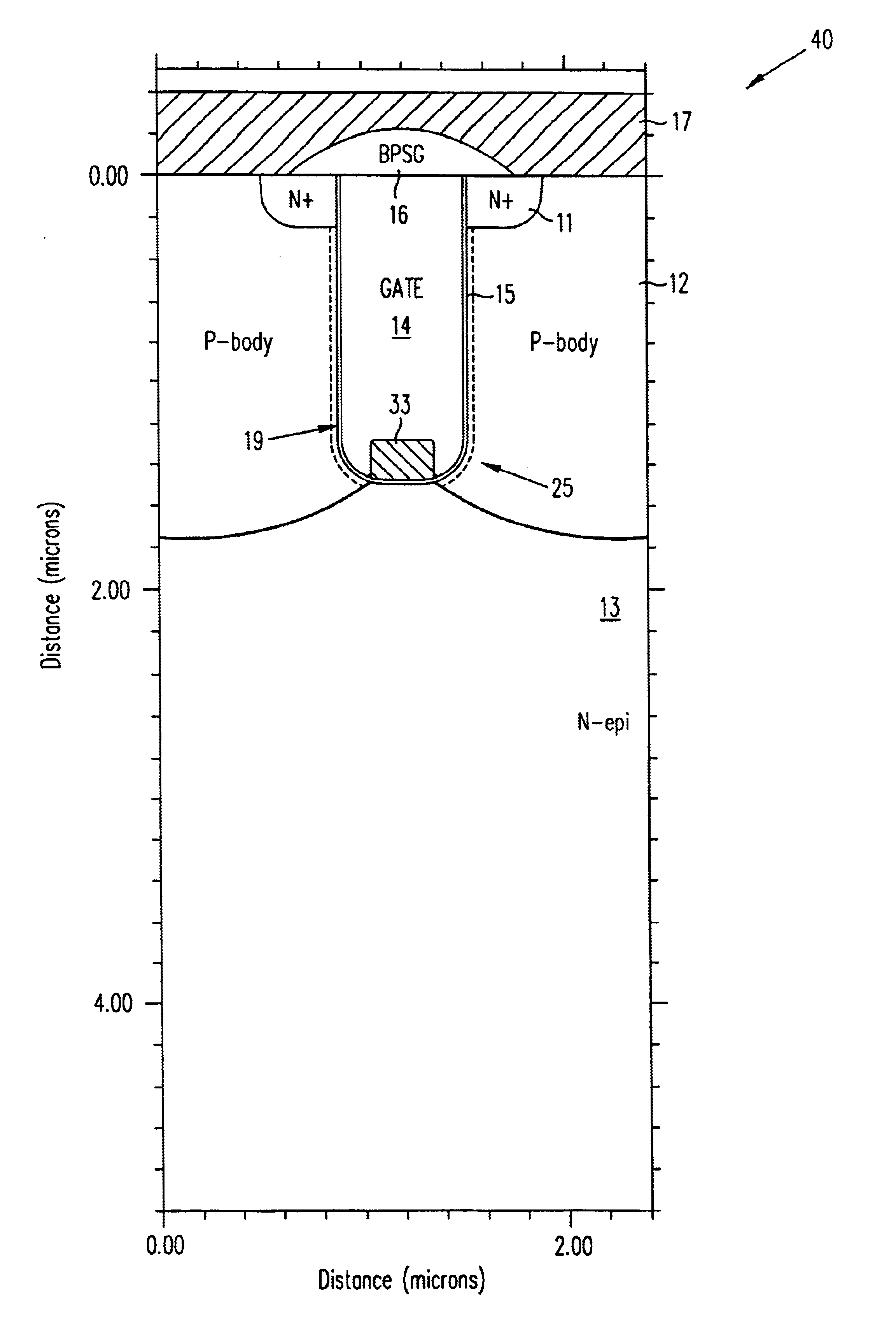
FIG. 4 is a cross-sectional view of one embodiment of a trench MOSFET 40 in accordance with the present invention. In MOSFET 40, an n-type epitaxial (“N-epi”) layer 13, which may be an N− layer and is usually grown on an N+ substrate (not shown), is the drain. A p-type body region 12 separates N-epi layer 13 from N+ source regions 11. Body region 12 is diffused along the sidewall of a trench 19, past a corner region 25, and partially long the bottom of trench 19. Current flows vertically through a channel (denoted by the dashed lines) along the sidewall and around corner region 25 of trench 19.

The sidewall and corner region 25 of trench 19 are lined with a thin gate insulator 15 (e.g., silicon dioxide). An oxide plug 33 is centrally located in the bottom of trench 19. Trench 19 is filled with a conductive material, such as doped polysilicon, which forms a gate 14. Gate 14 extends into corner region 25 of trench 19, between oxide plug 33 and gate insulator 15. Trench 19, including ga...


PUM


Abstract

Trench MOSFETs including active corner regions and a thick insulative layer at the bottom of the trench are disclosed, along with methods of fabricating such MOSFETs. In an exemplary embodiment, the trench MOSFET includes a thick insulative layer centrally located at the bottom of the trench. A thin gate insulative layer lines the sidewall and a peripheral portion of the bottom surface of the trench. A gate fills the trench, adjacent to the gate insulative layer. The gate is adjacent to the sides and top of the thick insulative layer. The thick insulative layer separates the gate from the drain conductive region at the bottom of the trench yielding a reduced gate-to-drain capacitance making such MOSFETs suitable for high frequency applications.

Description

FIELD OF THE INVENTIONThis invention relates to trench metal-insulator-semiconductor (MIS) devices and in particular to trench MOSFETs that are suitable for high frequency operation.BACKGROUNDSome metal-insulator-semiconductor (MIS) devices include a gate located in a trench that extends downward from the surface of a semiconductor substrate (e.g., silicon). The current flow in such devices is primarily vertical and, as a result, the cells can be more densely packed. All else being equal, this increases the current carrying capability and reduces the on-resistance of the device. Devices included in the general category of MIS devices include metal-oxide-semiconductor field effect transistors (MOSFETs), insulated gate bipolar transistors (IGBTs), and MOS-gated thyristors.Trench MOSFETs, for example, can be fabricated with a high transconductance (gm,max) and low specific on resistance (Ron), which are important for optimal linear signal amplification and switching. One of the most im...

Claims


Application Information

Patent Timeline
Patent Type & Authority Patents(United States)
IPC IPC(8): H01L21/02H01L29/423H01L29/66H01L21/28H01L21/336H01L29/40H01L29/78H01L29/49H01L29/02H01L29/08H01L29/06H01L29/51
CPCH01L21/28185H01L21/28238H01L29/0634H01L29/7834H01L29/4983H01L29/512H01L29/518H01L29/66621H01L29/7813H01L29/42368H01L21/28194H01L21/28211H01L29/0847H01L29/0878
Inventor DARWISH, MOHAMED N.GILES, FREDERICK P.LUI, KAM HONGCHEN, KUO-INTERRILL, KYLE
Owner SILICONIX
Why Eureka
Try Eureka