Semiconductor package with heat sink attached to substrate

a technology of heat sink and substrate, which is applied in the direction of semiconductor devices, semiconductor/solid-state device details, electrical apparatus, etc., can solve the problems of affecting the trace routability of the substrate, dislocation of the heat sink, and damage to the attachment between the heat sink and the substrate via adhesive or solder, so as to eliminate chip cracks and less damage to the substrate. , the effect of reducing the damag

Inactive Publication Date: 2005-02-01
SILICONWARE PRECISION IND CO LTD
View PDF10 Cites 48 Cited by
  • Summary
  • Abstract
  • Description
  • Claims
  • Application Information

AI Technical Summary

Benefits of technology

The above semiconductor package yields significant benefits in the use of a plurality of flexible clip members to clamp the substrate and the flange of the heat sink mounted on a surface of the substrate so as to secure the heat sink on the substrate in position. The edge of the substrate and / or the edge of the flange is formed with a plurality of grooves to be engaged with the clip members, such that the substrate and the heat sink can be clamped by the clip members. Moreover, the grooves of the substrate are preferably situated at positions corresponding to space between adjacent solder balls (implanted on a surface of the substrate opposite to the substrate mounted with the heat sink), thereby not affecting arrangement of the solder balls or ball pads (where the solder balls are bonded) on the substrate, and thus making the substrate capable of being mounted with a full array of solder balls. This method of positioning the heat sink on the substrate can eliminate chip cracks caused by directly coupling the heat sink onto the chip as in the prior art. Further, compared to the prior art of using fixing members (such as bolts) for attaching the heat sink to the substrate in which the heat sink and the substrate are formed with holes for being engaged with the fixing members, this feature of hole formation is not required in the semiconductor package according to the invention and thus trace routability on the substrate would not be affected. And, the grooves formed at the edge of the substrate only need to be dimensioned sufficiently to receive the clip members, thereby leading to much less damage to the substrate as compared to formation of holes on the substrate. In addition, the substrate free of holes can prevent damage from external moisture or contaminant entering into the holes and thereby eliminates the reliability issues to the semiconductor package.

Problems solved by technology

Further, as to enhance electrical performances of the semiconductor package, at least one passive component can be mounted on the substrate, which however would decrease area on the substrate capable of being in contact with the heat sink, thereby making the heat sink relatively difficult to be firmly adhered and positioned onto the substrate and thus leading to dislocation of the heat sink; this situation becomes severe in the use of a large heat sink.
Moreover, attachment between the heat sink and the substrate via the adhesive or solder would be damaged by unsatisfactory cleanness of contact surfaces between the heat sink and the substrate, or by undesirable stress applied to the heat sink and the substrate; in this case, delamination may occur at an interface between the heat sink and the substrate, and as a result, the heat sink is dislocated.
Furthermore, when the substrate mounted with the heat sink is subject to external force such as vibration or shock, the heat sink may also be dislocated from the substrate.
However, this structure is defective that the chip may be damaged if improperly pressing the heat sink onto the chip; further, during a high temperature process or thermal cycle, due to mismatch in coefficient of thermal expansion (CTE) between the heat sink and the chip, the chip may suffer thermal stress and crack.
However, this mechanical method of attaching the heat sink onto the substrate renders significant problems.
One is that predetermined area on the substrate is required for forming the holes, which may affect trace routability on the substrate and make the substrate not able to be mounted with a full array of solder balls.
Besides, formation of the holes would undesirably increase fabrication costs and process complexity of the substrate.
Further, external moisture or contaminant may enter the holes of the substrate and thus degrade reliability of fabricated products.
Therefore, the problem to be solved herein is to securely position a heat sink on a substrate without leading to dislocation of the heat sink, damaging a chip mounted on the substrate or affecting trace routability on the substrate.

Method used


Image

  • Semiconductor package with heat sink attached to substrate
  • Semiconductor package with heat sink attached to substrate
  • Semiconductor package with heat sink attached to substrate

Examples


first preferred embodiment

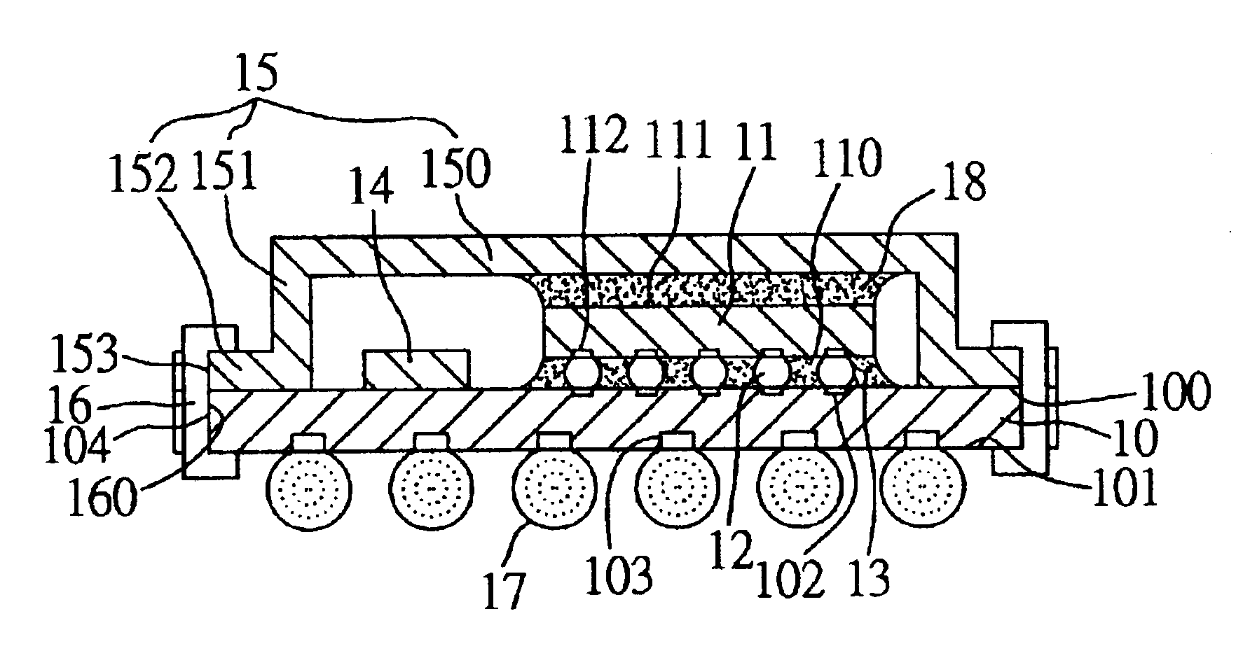
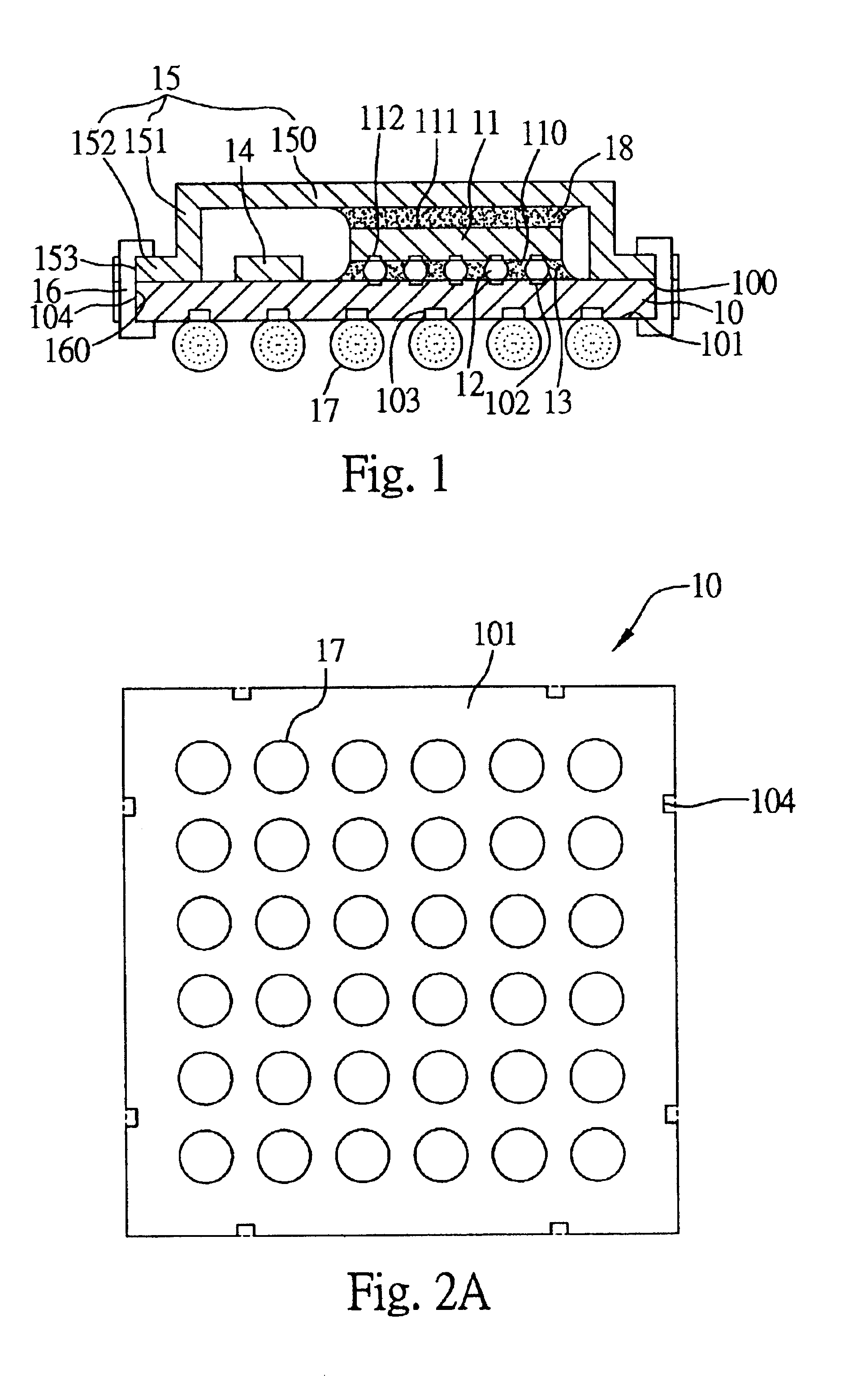
FIG. 1 illustrates a semiconductor package according to a first preferred embodiment of the invention. As shown in the drawing, this semiconductor package uses a substrate 10 as a chip carrier primarily made of a conventional resin material such as epoxy resin, polyimide resin, BT (Bismaleimide Triazine) resin, FR4 resin, etc.

The substrate 10 has an upper surface 100 and a lower surface 101 opposed to the upper surface 100. The upper surface 100 of the substrate 10 is formed with a plurality of bond pads 102 at predetermined positions where solder bumps 12 are bonded, and the lower surface 101 of the substrate 10 is formed with a plurality of ball pads 103 for being implanted with solder balls 17. The substrate 10 is fabricated by conventional processes which are not to be further detailed herein.

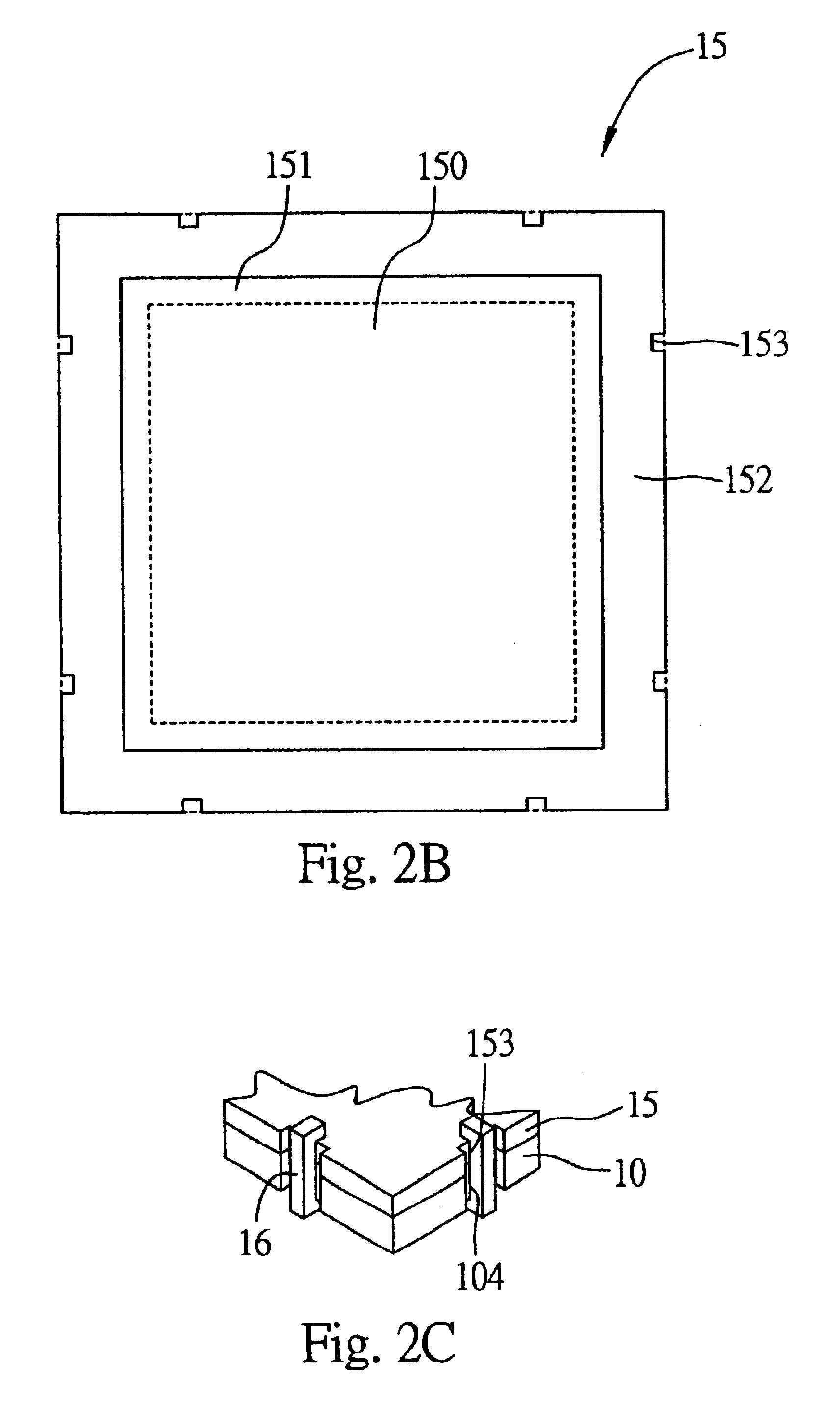
As shown in FIG. 2A, an edge of the substrate 10 is formed at predetermined positions with a plurality of inwardly recessed grooves 104 penetrating through the upper and lower surfaces 100,...

second preferred embodiment

FIG. 3 illustrates a semiconductor package according to a second preferred embodiment of the invention. As shown in the drawing, this semiconductor package is structurally similar to that of the first preferred embodiment, with the difference in that the flange 152 of the heat sink 15 is not formed with grooves; instead, coverage of the flange 152 is slightly smaller than that of the substrate 10, for example, the edge of the flange 152 being flush with dead ends of the grooves 104 of the substrate 10, such that the clip members 16 are engaged with the grooves 104 of the substrate 10 and clamp the heat sink 15 and the substrate 10.

third preferred embodiment

FIG. 4 illustrates a semiconductor package according to a third preferred embodiment of the invention. As shown in the drawing, this semiconductor package structurally differs from that of the first preferred embodiment in that the flange 152 of the heat sink 15 is attached to the upper surface 100 of the substrate 10 by means of an adhesive 19 so as to further firmly position the heat sink 15 on the substrate 10.

The above semiconductor package yields significant benefits in the use of a plurality of flexible clip members to clamp the substrate and the flange of the heat sink mounted on a surface of the substrate so as to secure the heat sink on the substrate in position. The edge of the substrate and / or the edge of the flange is formed with a plurality of grooves to be engaged with the clip members, such that the substrate and the heat sink can be clamped by the clip members. Moreover, the grooves of the substrate are preferably situated at positions corresponding to space between ...


PUM


Abstract

A semiconductor package with a heat sink is provided in which at least one chip is mounted on the substrate and covered by a heat sink. The heat sink is formed with a flange in contact with the substrate, allowing a plurality of clip members to clamp the flange of the heat sink and the substrate. Each of the clip members has a recess portion for receiving the flange of the heat sink and the substrate to thereby firmly position the heat sink on the substrate. The clip members are engaged with edges of the heat sink and the substrate, thereby not affecting trace routability on the substrate. Moreover, the heat sink is mounted on the substrate and would not be dislocated.

Description

FIELD OF THE INVENTIONThe present invention relates to semiconductor packages, and more particularly, to a semiconductor package with a heat sink for improving heat dissipating efficiency of the semiconductor package.BACKGROUND OF THE INVENTIONA FCBGA (flip-chip ball grid array) semiconductor package is formed with both a flip-chip structure and a ball grid array in which at least one chip is mounted and electrically connected to a surface of a substrate by a plurality of solder bumps, and a plurality of solder balls are implanted on an opposite surface of the substrate to serve as input / output (I / O) connections of the semiconductor package. In order to dissipate heat produced from operation of the chip, a heat sink is normally incorporated in the semiconductor package, as disclosed by U.S. Pat. Nos. 5,311,402, 5,637,920, 5,931,222 and 6,011,304. This heat sink is attached to the substrate by means of an adhesive or solder and is usually greater in surface area than the chip to cove...

Claims


Application Information

Patent Timeline
Patent Type & Authority Patents(United States)
IPC IPC(8): H01L23/367H01L23/34
CPCH01L23/3675H01L2224/16225H01L2224/32225H01L2224/73204H01L2224/73253H01L2924/15311H01L2924/16251H01L2924/19105H01L2924/00012H01L2924/00H01L2224/05571H01L2224/05573H01L2924/00014H01L2224/05599
Inventor LIN, CHANG-FUPU, HAN-PINGHSIAO, CHENG-HSUHUANG, CHIEN PING
Owner SILICONWARE PRECISION IND CO LTD
Why Eureka
Try Eureka