

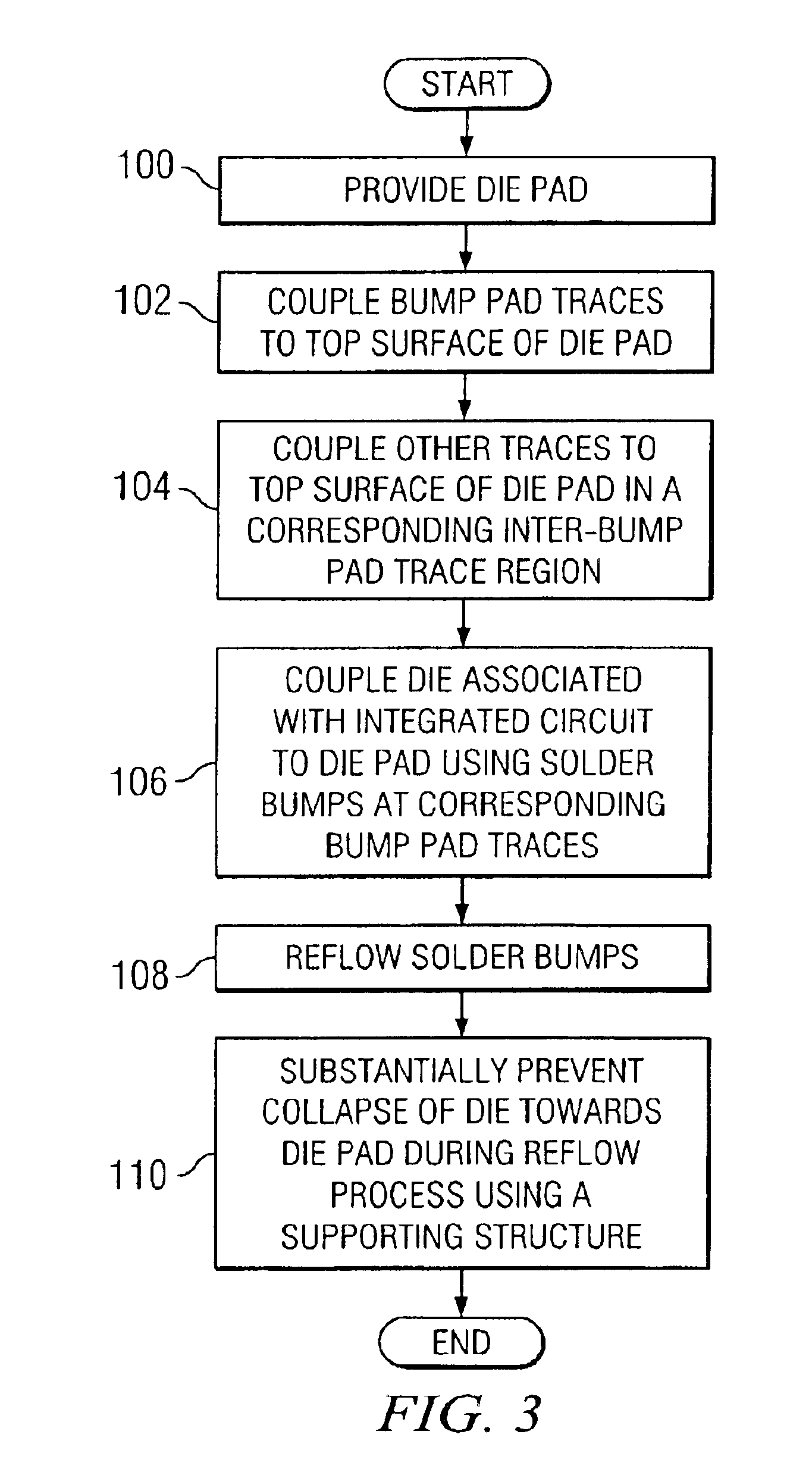
Using a supporting structure to control collapse of a die towards a die pad during a reflow process for coupling the die to the die pad
a technology of supporting structure and die pad, which is applied in the direction of printed circuit, sustainable manufacturing/processing, final product manufacturing, etc., can solve the problems of increasing costs and reducing manufacturing costs
- Summary
- Abstract
- Description
- Claims
- Application Information
AI Technical Summary
Benefits of technology
Problems solved by technology
Method used
Image

Examples
Embodiment Construction
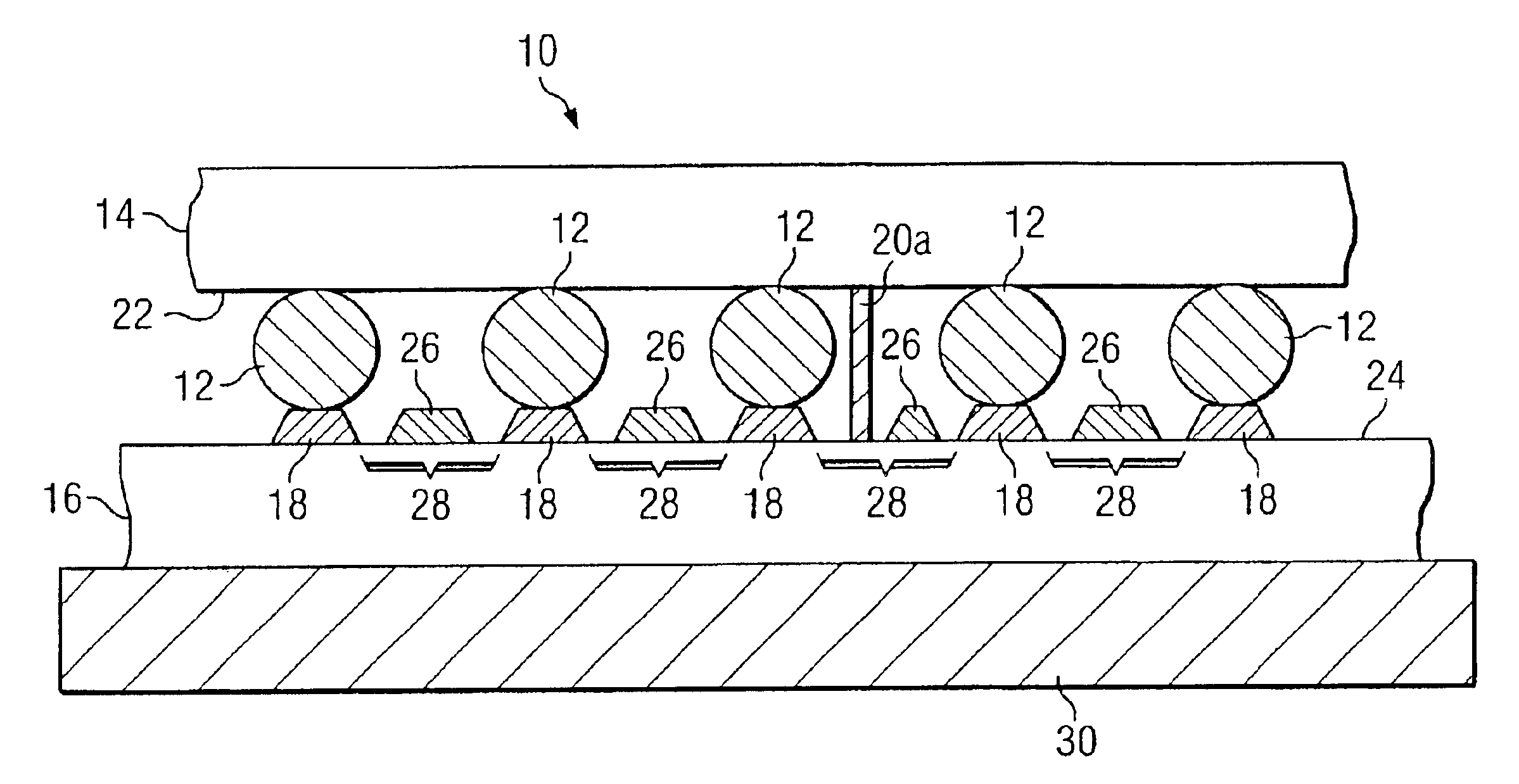
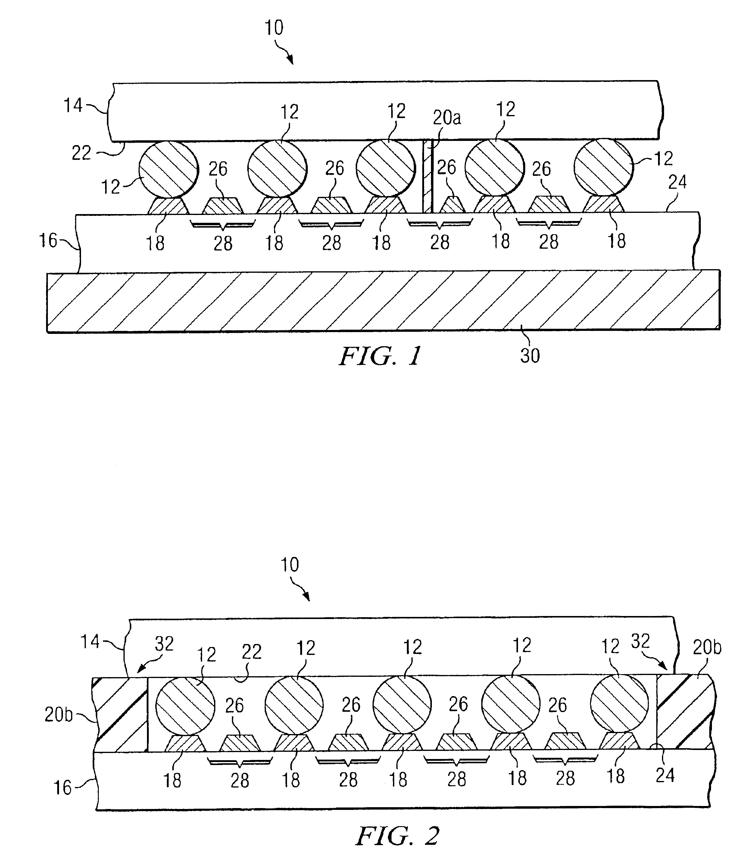
FIG. 1 illustrates a cross-sectional view of an example integrated circuit package 10 in which solder bumps 12 couple a die 14 to a die pad 16 at corresponding bump pad traces 18, one or more posts 20a that contact die 14 during the reflow process for bonding die 14 to die pad 16 having been used to substantially prevent collapse of die 14 towards die pad 16 during the reflow process. In one embodiment, integrated circuit package 10 includes a flip chip assembly, although the present invention contemplates integrated circuit package 10 including any suitable type of integrated circuit package in which one or more solder bumps or solder balls couple layers of the integrated circuit package. Reference to solder bumps is meant to include solder bumps, solder balls, or any other suitable structures.
Die 14 may be associated with an integrated circuit and has a bottom surface 22. Die 14 may have any suitable area and shape, according to particular needs. Die pad 16 has a top surface 24 op...
PUM
 Abstract
Description
Claims
Application Information