Semiconductor device capable of internally generating bias changing signal

a technology of bias change and semiconductors, applied in pulse manipulation, pulse techniques, instruments, etc., can solve the problems of increasing power consumption, burdening users, and another burden on users, and achieve the effect of reducing the burden on users

Inactive Publication Date: 2005-02-01
RENESAS ELECTRONICS CORP
View PDF7 Cites 14 Cited by
  • Summary
  • Abstract
  • Description
  • Claims
  • Application Information

AI Technical Summary

Benefits of technology

[0007]It is an object of the present invention to provide a sem

Problems solved by technology

That is, in a high access mode state, the bias currents are increased to increase the operation speed while the power consumption is increased.
In the above-described prior art semiconductor device, however, the bias changing signal in synchronization with the control signal has to be input as an external signal

Method used


Image

  • Semiconductor device capable of internally generating bias changing signal
  • Semiconductor device capable of internally generating bias changing signal
  • Semiconductor device capable of internally generating bias changing signal

Examples


first embodiment

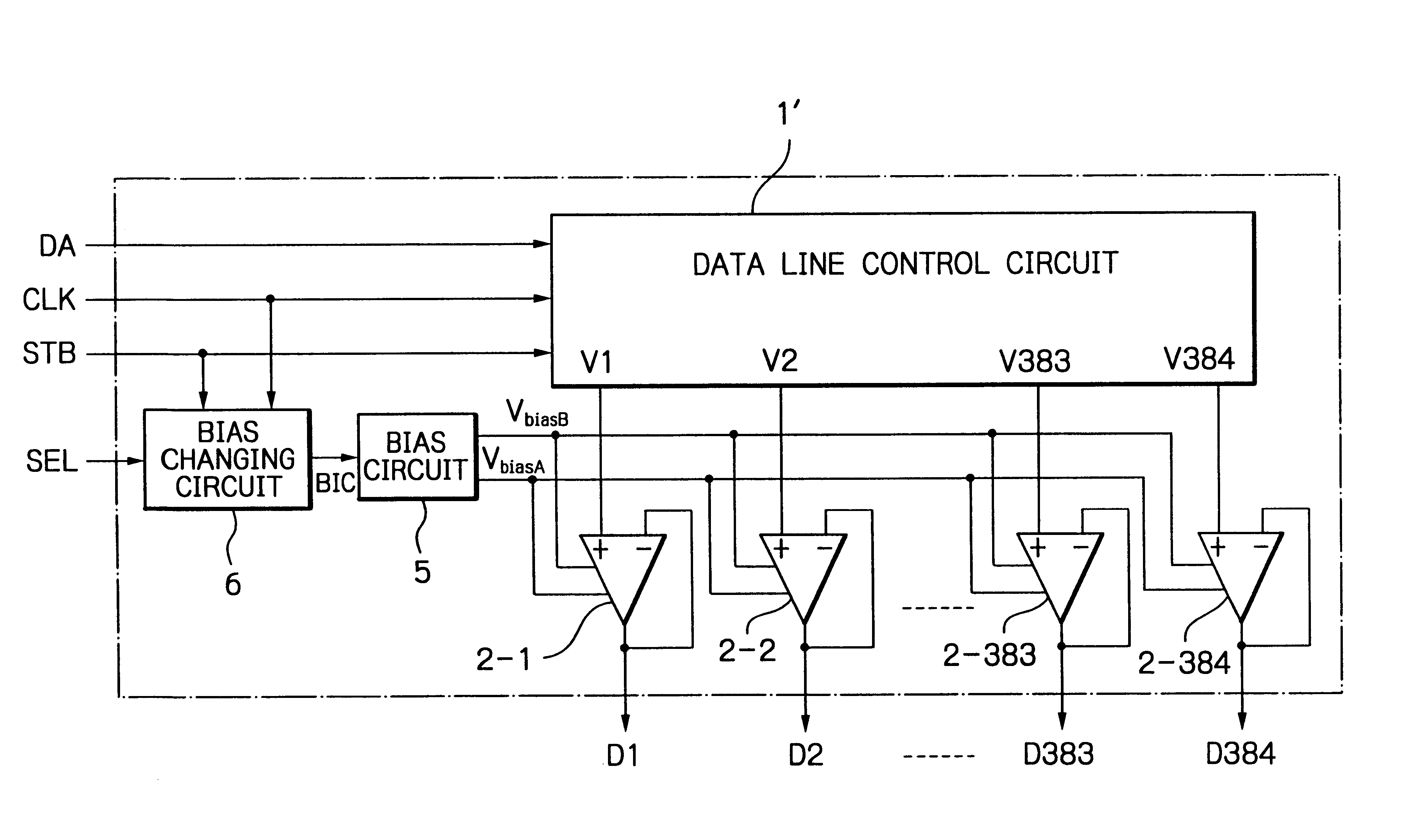
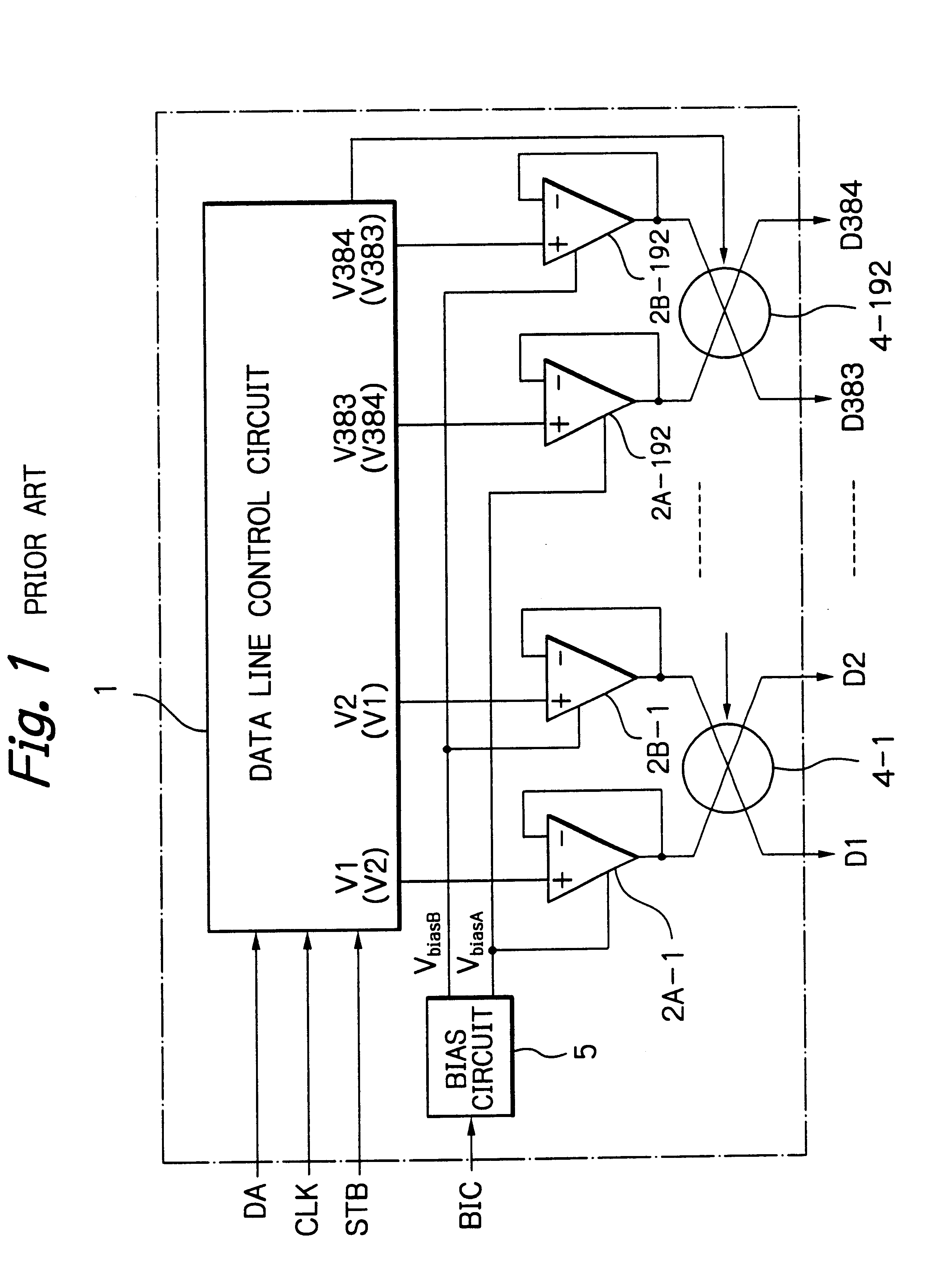
[0049]In FIG. 6, which illustrates the data line driver of an LCD apparatus according to the present invention, a bias changing circuit 6 is added to the elements of FIG. 1. The bias changing circuit 6 receives the strobe signal STB and the clock signal CLK to generate the bias changing signal BIC. That is, the bias changing signal BIC is internally generated. Also, the bias changing circuit 6 receives a selection signal SEL to change the predetermined time period of a high access mode (high power consumption mode) in accordance with the number of data lines and / or the fluctuation of the resistance and capacitance of an LCD panel. Note that since the selection signal SEL is set to be low or high, the selection signal SEL can be easily set by the user.

[0050]In FIG. 7, which is a detailed circuit diagram of the bias changing circuit 6 of FIG. 6, the bias changing circuit 6 is constructed by an 8-bit counter 61 for counting the pulses of the clock signal CLK, a 9-bit counter 62 for cou...

second embodiment

[0070]In FIG. 11, which illustrates the data line driver of an LCD apparatus according to the present invention, a bias changing circuit 6 of FIG. 6 is added to the elements of FIG. 4. Even in FIG. 11, the bias changing circuit 6 receives the strobe signal STB and the clock signal CLK to generate the bias changing signal BIC. That is, the bias changing signal BIC is internally generated. Also, the bias changing circuit 6 receives a selection signal SEL to change the predetermined time period of a high access mode (high power consumption mode) in accordance with the number of data lines and / or the fluctuation of the resistance and capacitance of an LCD panel. Note that since the selection signal SEL is set to be low or high, the selection signal SEL can be easily set by the user.

[0071]In the above-described embodiments, the counter 61 is an 8-bit counter and the counter 62 is a 9-bit counter, however, the counter 61 can be an m-bit (m=2, 3, . . . ) counter and the counter 62 can be a...


PUM


Abstract

In a semiconductor device, at least one operational amplifier drives a capacitive load in accordance with a control signal. A bias changing circuit receives the control signal to generate a bias changing signal in synchronization with the control signal dependent upon a width of the control signal. A bias circuit controls a bias current flowing through the operational amplifier in accordance with the bias changing signal.

Description

BACKGROUND OF THE INVENTION[0002]1. Field of the Invention[0003]The present invention relates to a semiconductor device such as a data line driver of a liquid crystal display (LCD) apparatus, and more particularly, to the improvement of generation of a bias changing signal for changing a bias current flowing through an operational amplifier (voltage follower) for driving a capacitive load.[0004]2. Description of the Related Art[0005]In a prior art semiconductor device such as a prior art data line driver of an LCD apparatus, a plurality of voltage followers are provided to drive a plurality of capacitive loads such data lines in accordance with a control signal such as a strobe signal. Also, a bias circuit controls bias currents flowing through the voltage followers in accordance with an externally-generated bias changing signal. That is, in a high access mode state, the bias currents are increased to increase the operation speed while the power consumption is increased. On the othe...

Claims


Application Information

Patent Timeline
IPC IPC(8): G09G3/36H03K5/24H03K5/22H03F1/02H03K5/003G11C5/14G09G3/20
CPCG09G3/3688H03K5/2481H03K5/003H03F1/0261G09G2310/027G11C5/14
Inventor TAZUKE, TOSHIKAZU
Owner RENESAS ELECTRONICS CORP
Why Eureka
Try Eureka