Semiconductor device and method for manufacturing the same

a technology of semiconductors and semiconductors, applied in the direction of semiconductor devices, electrical equipment, transistors, etc., can solve the problems of increased dose loss, achieve the effect of reliably improving the activation ratio of p-type impurity ions, reliably preventing the dose loss phenomenon, and suppressing the production of bics

Inactive Publication Date: 2005-02-08
TAIWAN SEMICON MFG CO LTD
View PDF9 Cites 28 Cited by
  • Summary
  • Abstract
  • Description
  • Claims
  • Application Information

AI Technical Summary

Benefits of technology

In the method for manufacturing a semiconductor device of the present invention, it is preferred that the second step includes implanting ion of the group IV element at a dose equal to or greater than a dose such that the semiconductor region is turned into an amorphous state. In this way, it is possible to uniformly form the a/c interface at a position shallower than the junction plane of the extension high concentration diffusion layer.
In the method for manufacturing a semiconductor device of the present invention, it is preferred that the third step includes implanting the second impurity with an implantation projected range of about 14 nm or less. Thus, the second impurity can be implanted at a low energy so as to provide a shallow junction, and the dose loss phenomenon in the extension high concentration diffusion layer can still be suppressed by the dislocation loop defect layer. Therefore, it is possible to reliably locate the junction plane of the extension high concentration diffusion layer at a shallow position.
In the method for manufacturing a semiconductor device of the present invention, it is preferred that the second impurity is a molecule containing boron fluoride or fluorine. In this way, since the fluorine atoms are likely to be captured by the dislocation loop defect layer, a strong flux of fluorine atoms toward the surface side of the semiconductor region can be reduced, whereby it is possible to reliably prevent the dose loss phenomenon of P-type impurity ion such as boron ion.
In the method for manufacturing a s

Problems solved by technology

Another problem is that the dose loss increases as the boron fluoride im

Method used


Image

  • Semiconductor device and method for manufacturing the same
  • Semiconductor device and method for manufacturing the same
  • Semiconductor device and method for manufacturing the same

Examples


first embodiment

A first embodiment of the present invention will be described with reference to the drawings.

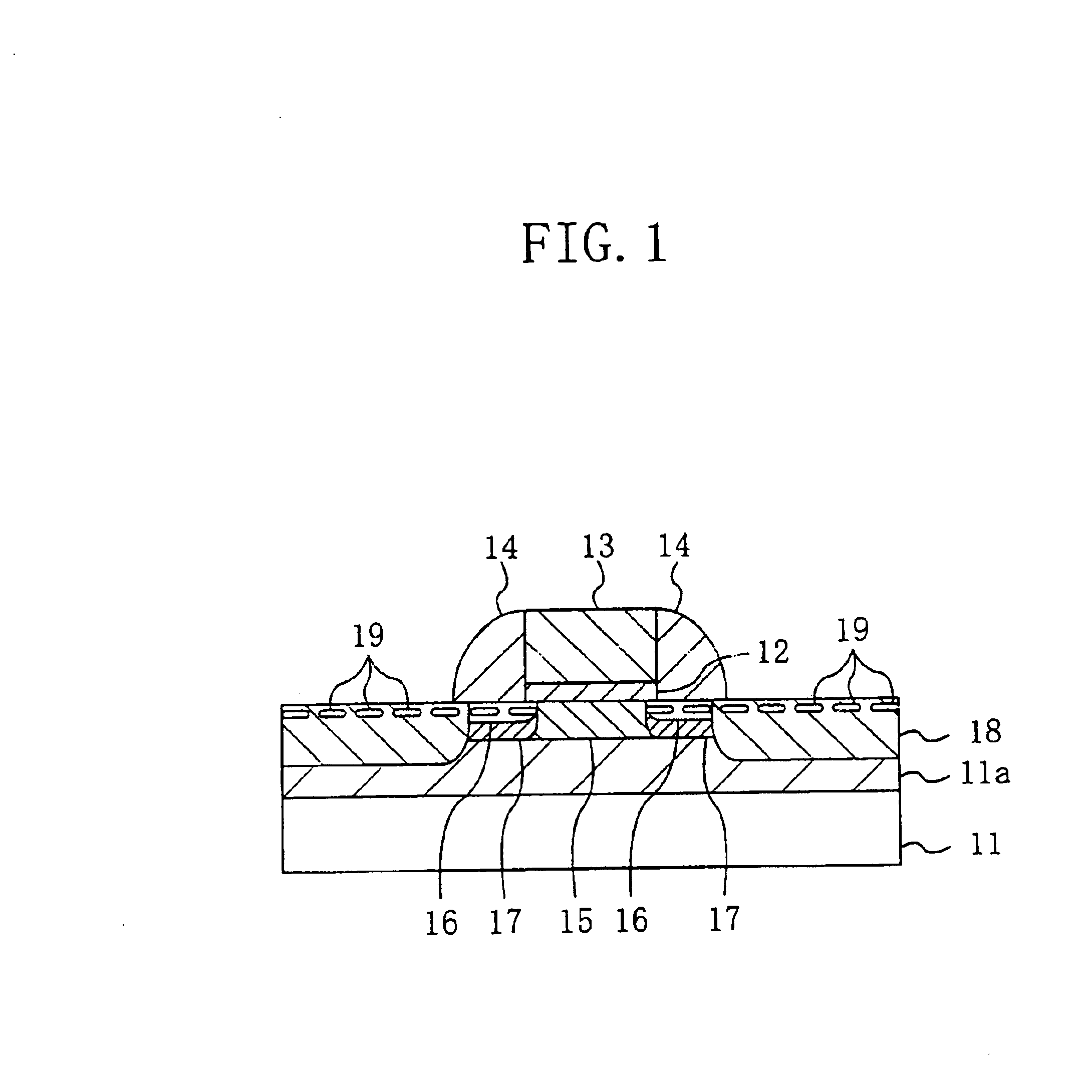
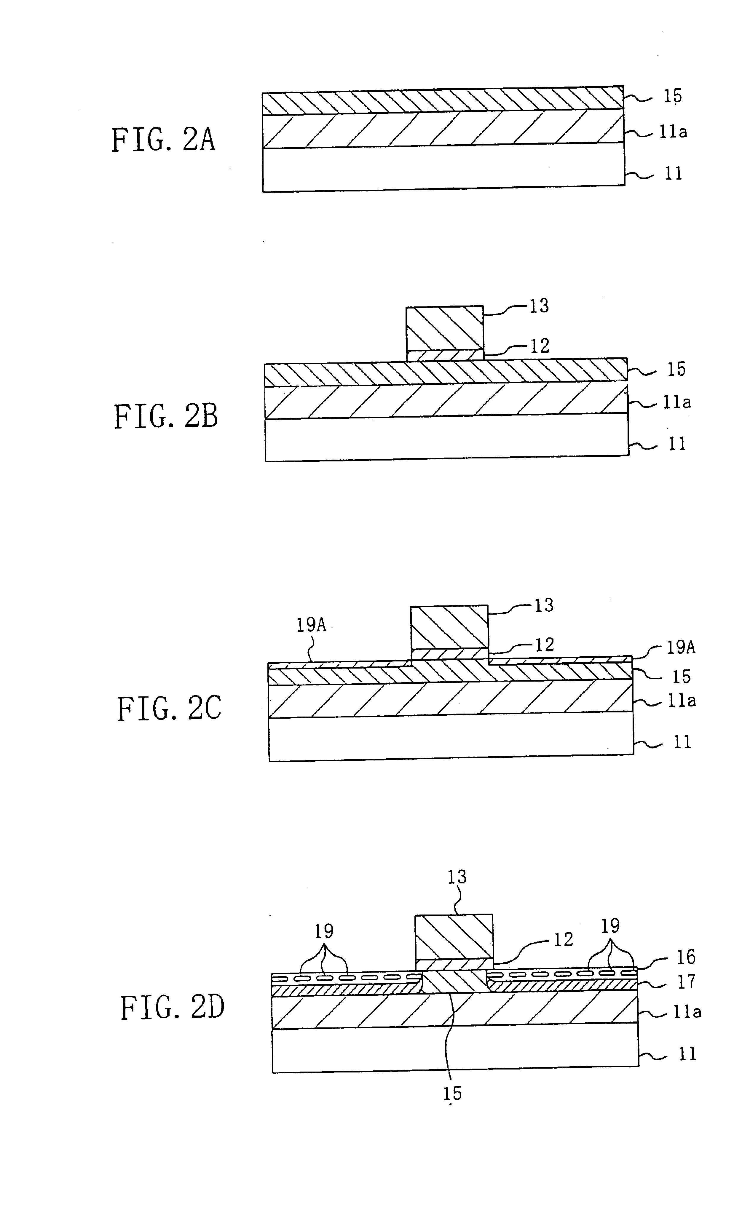
FIG. 1 is a cross-sectional view illustrating an MIS transistor according to the first embodiment of the present invention.

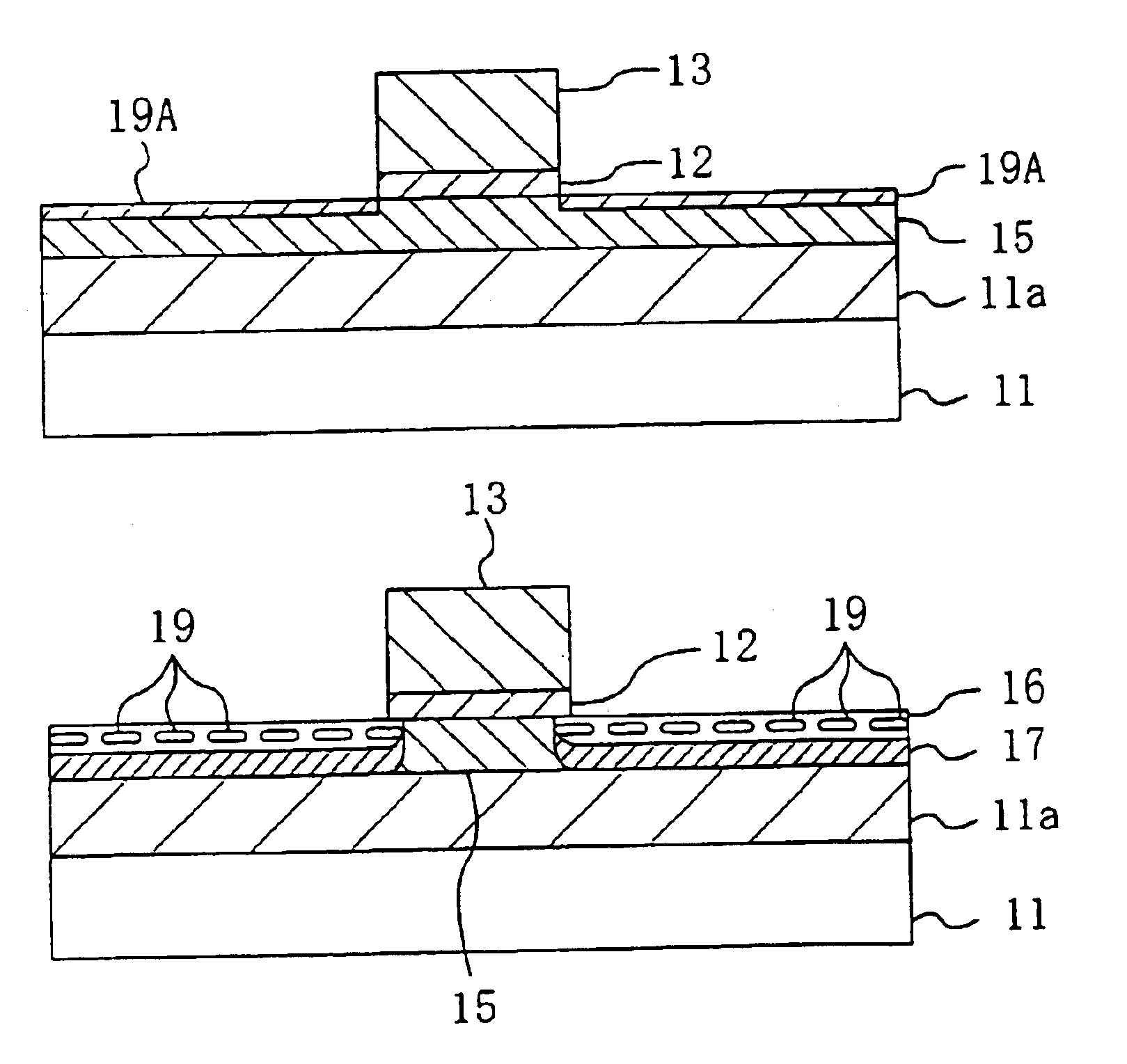
As illustrated in FIG. 1, an N-type well 11a is formed in an upper portion of a semiconductor substrate 11 made of P-type silicon, for example. Note that while the transistor of the present embodiment is formed in and on the N-type well 11a, the N-type well 11a may alternatively an N-type semiconductor layer provided in a substrate having an SOI structure, or an N-type semiconductor substrate may alternatively be used.

A gate electrode 13 made of poly-metal or polysilicon is selectively formed on the N-type well 11a via a gate insulative film 12 made of silicon oxide, or the like. A side wall 14 made of silicon nitride or silicon oxide is formed on a side surface of the gate electrode 13.

An N-type channel diffusion layer 15 is formed in a region of the N-type well 11a bel...

second embodiment

A second embodiment of the present invention will now be described with reference to the drawings.

FIG. 6A to FIG. 6D and FIG. 7A to FIG. 7C are cross-sectional views sequentially illustrating steps in a method for manufacturing an MIS transistor according to the second embodiment of the present invention.

First, referring to FIG. 6A, the semiconductor substrate 11 made of P-type silicon is subjected to ion implantation at an implantation energy of about 140 keV and a dose of about 1×10¹² / cm2 by using N-type impurity ion, e.g., arsenic ion. Then, using N-type impurity ion, e.g., phosphorus ion, ion implantation at an implantation energy of about 260 keV and a dose of about 4×10¹² / cm2 is performed, and further ion implantation at an implantation energy of about 540 keV and a dose of about 1×10¹³ / cm2 is performed. Following the ion implantation, rapid thermal annealing is performed, in which the intermediate product is heated to a high temperature of about 900° C. to about 1025° C. at a...

third embodiment

A third embodiment of the present invention will now be described with reference to the drawings.

FIG. 8A to FIG. 8D, FIG. 9A and FIG. 9B are cross-sectional views sequentially illustrating steps in a method for manufacturing an MIS transistor according to the third embodiment of the present invention.

First, referring to FIG. 8A, the semiconductor substrate 11 made of P-type silicon is subjected to ion implantation at an implantation energy of about 140 keV and a dose of about 1×10¹² / cm2 by using N-type impurity ion, e.g., arsenic (As) ion. Then, using N-type impurity ion, e.g., phosphorus (P) ion, ion implantation at an implantation energy of about 260 keV and a dose of about 4×10¹² / cm2 is performed, and further ion implantation at an implantation energy of about 540 keV and a dose of about 1×10¹³ / cm2 is performed. Following the ion implantation, rapid thermal annealing is performed, in which the intermediate product is heated to a high temperature of about 900° C. to about 1025° C....


PUM


Abstract

A semiconductor device includes a gate electrode formed on a semiconductor region via a gate insulative film and an extension high concentration diffusion layer of a first conductivity type formed in the semiconductor region beside the gate electrode. A dislocation loop defect layer is formed in a region of the semiconductor region beside the gate electrode and at a position shallower than an implantation projected range of the extension high concentration diffusion layer.

Description

BACKGROUND OF THE INVENTIONThe present invention relates to a semiconductor device capable of operating at a high speed with a low power consumption and with which it is possible to further increase the degree of integration of semiconductor integrated circuits, and a method for manufacturing the same.With the advent of ultra high scale integration of semiconductor integrated circuits, there has been a growing demand in the art for further miniaturization of MIS transistors. A method for manufacturing an MIS transistor having a shallow junction plane is desired for realizing the further miniaturization of MIS transistors.A conventional method for manufacturing an MIS transistor will now be described with reference to the drawings.First, referring to FIG. 13A, arsenic (As) ion, which is an N-type impurity, and phosphorus (P) ion, for which the implantation energy and the dose are greater than those for the arsenic ion, are implanted into a semiconductor substrate 101 made of P-type s...

Claims


Application Information

Patent Timeline
IPC IPC(8): H01L21/265H01L21/02H01L21/336
CPCH01L21/26506H01L29/6659H01L21/26513H01L21/26566H01L21/2658
Inventor NODA, TAIJI
Owner TAIWAN SEMICON MFG CO LTD
Why Eureka
Try Eureka