Reducing jitter in mixed-signal integrated circuit devices
- Summary
- Abstract
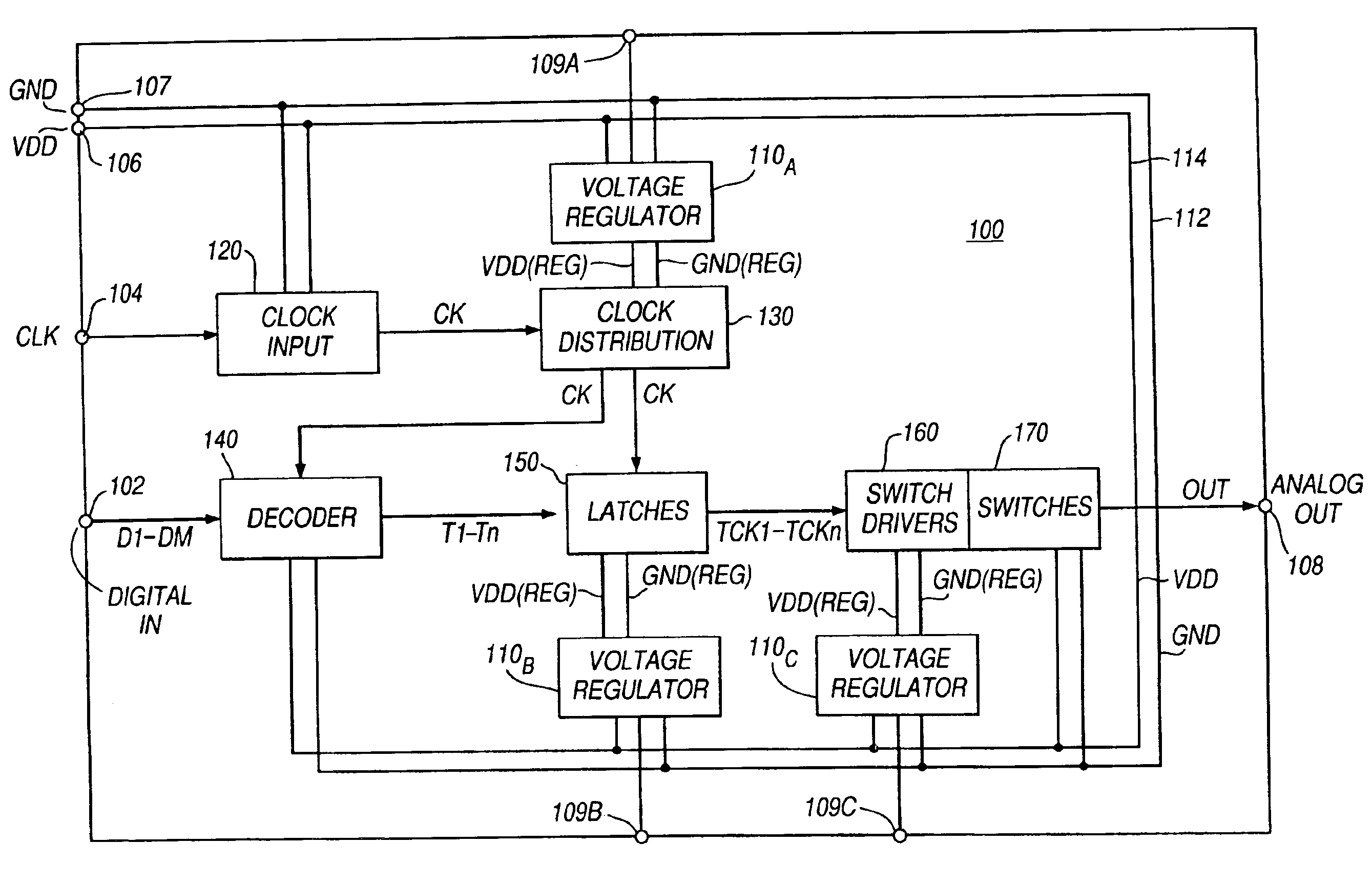
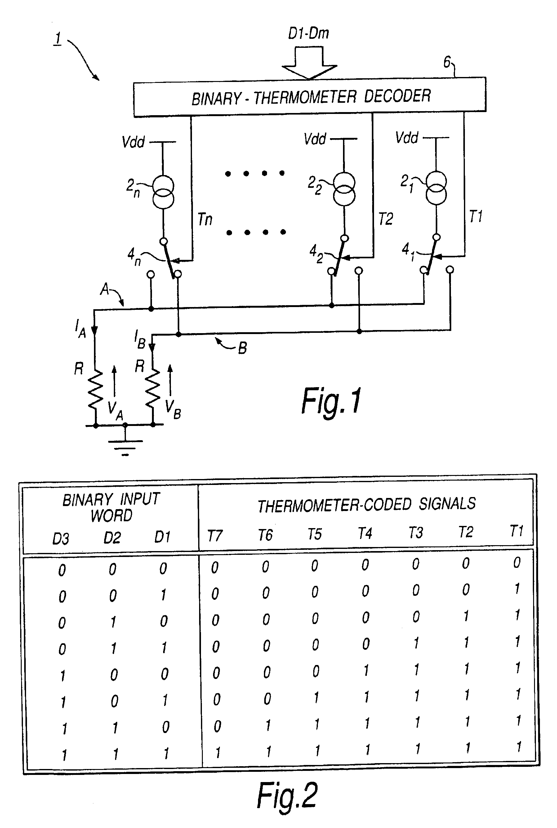
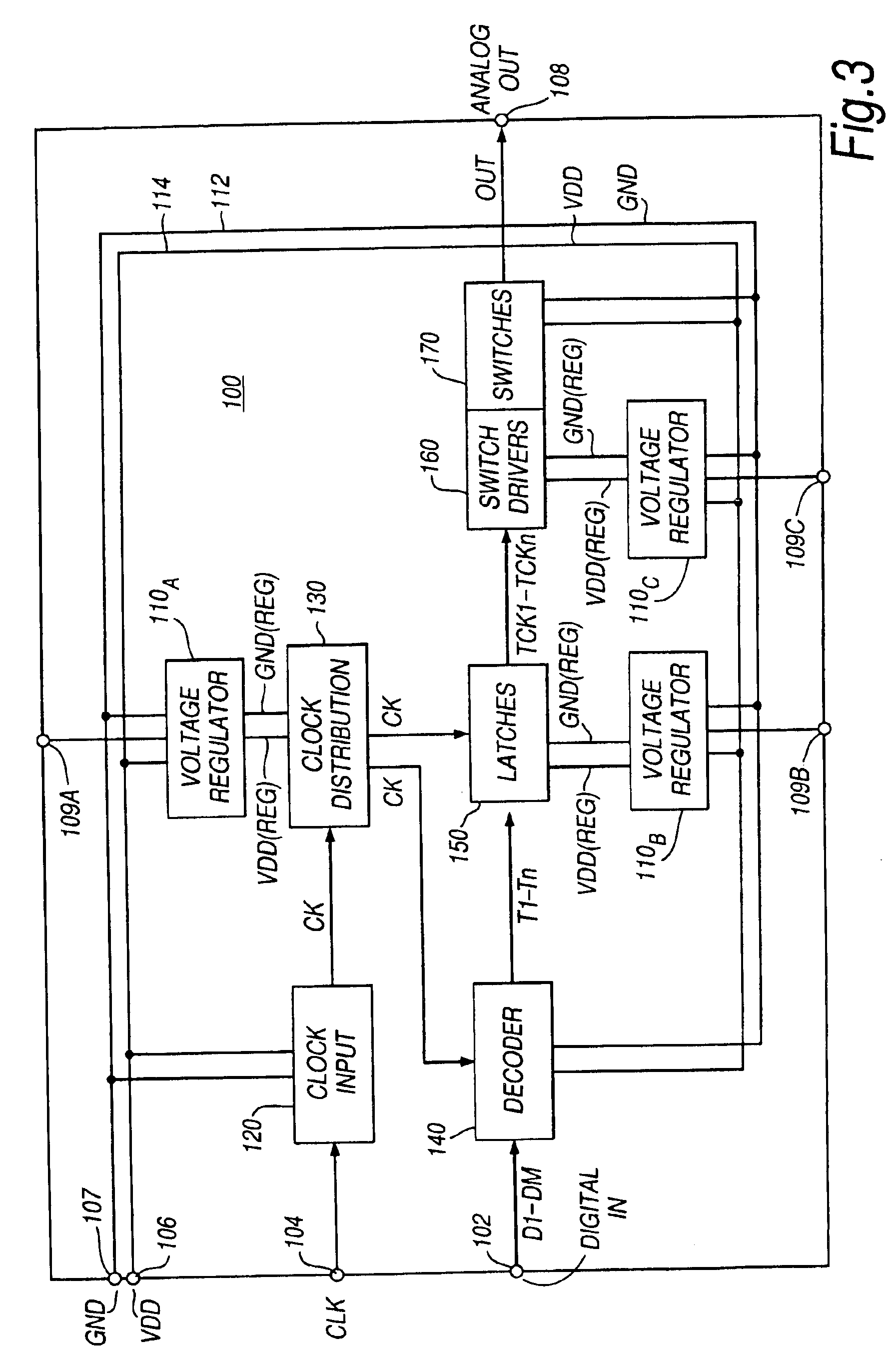
- Description
- Claims
- Application Information
AI Technical Summary
Problems solved by technology
Method used
Image

Examples
Embodiment Construction
Before a detailed description of embodiments of the present invention, further considerations relating to the problems mentioned above with regard to jitter caused by power supply variation will first be discussed.
For circuits in which delay is a function of supply voltage and which are required to exhibit very low jitter characteristics, very low-noise power supplies are required. This is particularly true for CMOS circuits, where the delay is approximately proportional to the square root of the supply voltage, which operate at high frequencies with low jitter (for example, high-speed ADCs and DACs) and where the delay from clock to output is not very small (for example, in a case where the clock signal is distributed through a tree-form circuit which results in delays).
For example, consider the case of a DAC producing as its analog output signal a sinewave having an amplitude of 1 V and a frequency Fout of 100 MHz, the DAC having a 1 ns total delay from its clock input to its diff...
PUM
 Abstract
Description
Claims
Application Information