Semiconductor device and method of manufacturing semiconductor device

a semiconductor and semiconductor technology, applied in semiconductor devices, semiconductor/solid-state device details, electrical apparatus, etc., can solve the problems of failure of the function of a semiconductor element, increased manufacturing cost, and difficulty in using the step of forming an insulating layer by thermal oxidation treatment, etc., to achieve reliable electrical conduction, low cost, and high aspect ratio

Inactive Publication Date: 2005-02-15
CANON KK
View PDF16 Cites 122 Cited by
  • Summary
  • Abstract
  • Description
  • Claims
  • Application Information

AI Technical Summary

Benefits of technology

In view of the above-described circumstances, an object of the present invention is to provide at a low cost a semiconductor device in which reliable electrical conduction is provided between front and back surfaces of a substrate. Another object of the present invention is to provide an improved semiconductor device using a through hole with a high aspect ratio and a small diameter as accompanying the tendency toward improvements in degree of integration and packaging density.

Problems solved by technology

In a case where through holes are formed in a semiconductor device for electrical conduction between front and back surfaces, if semiconductor elements or electrode pads electrically connected to semiconductor elements are formed after the formation of the through holes, there is a need to again form a wiring pattern or the like after the formation of the semiconductor elements or the electrode pads and the manufacturing process becomes complicated, resulting in an increase in manufacturing cost.
It is known that in ordinary cases a failure can occur in the function of a semiconductor element when the semiconductor element is subjected to a high temperature of 600° C. or higher.
Therefore it is difficult to use a step of forming an insulating layer by a thermal oxidation treatment in a case where semiconductor elements and electrode pads are formed on a semiconductor substrate in advance.
However, it is difficult to use thermal CVD among chemical vapor deposition methods in a case where semiconductor elements and electrode pads are formed on a substrate in advance, since thermal CVD ordinarily requires heating at a high temperature of 600° C. or higher, as in the case of the above-mentioned thermal oxidation treatment.
In a case where the inside surface of a through hole in a substrate is made electroconductive, for example, for the reason that the substrate is electroconductive, a leak occurs between the electroconductive semiconductor substrate and an electroconductive layer formed on the inside surface of the insulating layer, resulting in failure in the functions of the semiconductor device using the substrate.
The forming speed of an insulating layer in a through hole is extremely small in comparison with that at the front and back surfaces of a semiconductor substrate, since the gas cannot easily enter the through hole and cannot circulate well.
Thus, it is difficult to efficiently form an insulating layer on the inside surface of a through hole.
It is also difficult to maintain the uniformity of formed layer.
In particular, it is extremely difficult to form, by chemical vapor deposition, a uniform layer in a through hole of a semiconductor chip for ordinarily use when the aspect ratio is 5 or higher or when the inside diameter is 100 μm or smaller.
Thus, in some cases, there is high possibility of failure to insulate an inner portion of a through hole due to the existence of a defective portion of an insulating layer.

Method used


Image

  • Semiconductor device and method of manufacturing semiconductor device
  • Semiconductor device and method of manufacturing semiconductor device
  • Semiconductor device and method of manufacturing semiconductor device

Examples


embodiment 1

(Embodiment 1)

A semiconductor device and a manufacturing method which represent Embodiment 1 of the present invention will be described with reference to FIG. 1, FIG. 2, and FIGS. 3A through 3G.

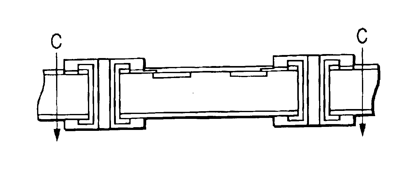
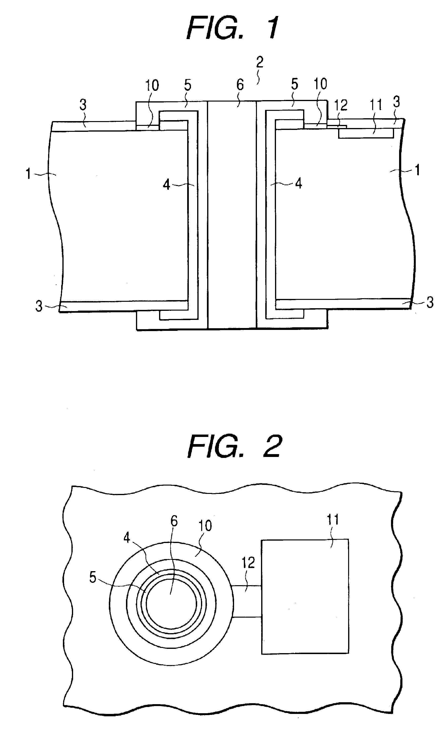
FIG. 1 is a schematic cross-sectional view of a portion of a substrate of the semiconductor device according to Embodiment 1 in which a through hole is formed, and FIG. 2 is a top perspective view of the substrate, showing an internal portion for ease of explanation. The substrate of the semiconductor device is indicated by 1. A through hole 2 is formed through the substrate 1 between front and back surfaces of the substrate. A protective layer 3 is formed on each of the front and back surfaces of the substrate. An insulating layer 4 of an organic material is formed on the inner surface of the through hole 2, and on the front and back surfaces of the substrate 1 around the opening ends of the through hole 2. An electroconductive layer 5 is formed on the inner surface so as to cover the insula...

example 1

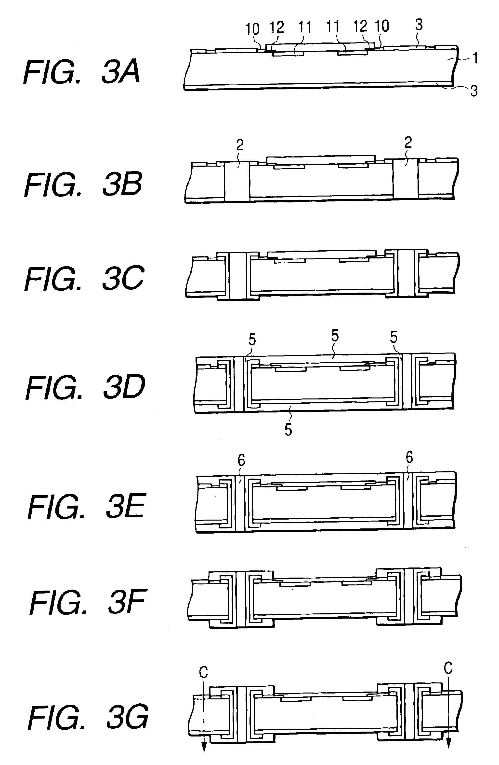
Examples of the present invention according to the above-described Embodiment 1 will be described. In Example 1, a semiconductor device was formed according to the form shown in FIG. 1.

First, in a step corresponding to that shown in FIG. 3A, a 6-inch substrate 1 which is a silicon semiconductor substrate is prepared. Electrode pads 10, a semiconductor elements 11 and wiring conductors 12 are provided on a surface of the substrate 1 in advance. Portions other than the electrode pads 10 are covered with a protective layer 3. The thickness of the electrode pad 10 is 0.21 μm and the thickness of the wiring conductor 12 is 0.5 μm. The protective layer 3 is formed of a multilayer of SiO2 and SiN. The thickness of substrate 1 is 625 μm. When these members are formed, an insulating film (not shown) having a thickness of about 0.1 μm is formed between the electrode pad 10 and the substrate 1 and between the wiring conductor 12 and the substrate 1.

Thereafter, in a step corresponding to that s...

embodiment 2

(Embodiment 2)

Embodiment 2 of the present invention will be described with reference to FIG. 7. In FIG. 7, members identical or corresponding to those shown in FIG. 1 are indicated by the same reference characters. FIG. 7 illustrates a substrate 1, a through hole 2, a protective layer 3, an insulating layer 4, an electroconductive layer 5, a filling material 6, an electrode pad 10, a semiconductor element 11, and a wiring conductor 12. In the above-described Embodiment 1, the insulating layer 4 is formed on the inside surface of the through hole 2 and on the front and back surfaces of the substrate 1 around the opening ends of the through hole 2. In this embodiment, the insulating layer 4 is formed only on the inside surface of the through hole 2. The insulating layer 4 in this embodiment is formed in such a manner that a masking insulating film is formed on the protective layer 3 before the insulating layer 4 is formed, and the masking insulating film is peeled off after the format...


PUM


Abstract

The semiconductor device of the present invention comprises a substrate; at least one through hole formed through the substrate between front and back surfaces of the substrate; an electrical connection portion formed by a semiconductor process on at least one surface of the front and back surfaces of the substrate in a vicinity of an end opening of the through hole; an insulating layer formed of an organic material on an inside surface of the through hole; and an electroconductive layer formed on an inside surface of the insulating layer, wherein the electrical connection portion is electrically connected to the electroconductive layer to be electrically connected to a side of the other surface of the substrate.

Description

BACKGROUND OF THE INVENTION1. Field of the InventionThe present invention relates to a semiconductor device having semiconductor elements formed on its surface and to a method of manufacturing the semiconductor device.2. Related Background ArtSemiconductor devices have been formed in such a manner that wiring and electrode pads are formed on a substrate such as a semiconductor substrate or a glass substrate by a semiconductor process, and a plurality of semiconductor chips are mounted on the surface of the substrate. With the miniaturization of semiconductor devices, there has been an increased need to reduce the size of the semiconductor devices and to increase the mounting density. To meet this need, connections from the back surface of a substrate to external terminals are made by providing electrical conduction between the front and back surfaces of the substrate, the back surface of the substrate is used for wiring by providing electrical conduction between the front and back s...

Claims


Application Information

Patent Timeline
Patent Type & Authority Patents(United States)
IPC IPC(8): H01L21/70H01L23/48H01L21/768H01L23/52H01L21/3205
CPCH01L21/76898H01L23/481H01L2924/09701H01L2924/12044H01L2924/0002H01L2924/00H01L2224/02371H01L21/60
Inventor MUTA, TADAYOSHITACHIKAWA, JINSAITO, RIICHISUTO, TADANORITAKAYAMA, MANABUMORIMOTO, HIROYUKI
Owner CANON KK
Why Eureka
Try Eureka