High-frequency multilayer circuit substrate

a multi-layer circuit and substrate technology, applied in the direction of high-frequency circuit adaptation, waveguide, waveguide type devices, etc., can solve the problems of signal wave reflection in the transmission line, increased manufacturing cost, and increased transmission loss

Inactive Publication Date: 2005-02-15
SHARP KK
View PDF12 Cites 45 Cited by
  • Summary
  • Abstract
  • Description
  • Claims
  • Application Information

AI Technical Summary

Benefits of technology

According to the high-frequency multilayer circuit substrate of the above-mentioned embodiments, the characteristic impedance of the via hole connecting portion is eas

Problems solved by technology

As reduction in size and increase in transmission signal frequency of this multilayer circuit substrate have been needed, a transmission loss due to signal wave reflection in the transmission lines and a via hole connecting portion has become a more serious trouble.
However, in terms of a substrate manufacturing proces

Method used


Image

  • High-frequency multilayer circuit substrate
  • High-frequency multilayer circuit substrate
  • High-frequency multilayer circuit substrate

Examples


second embodiment

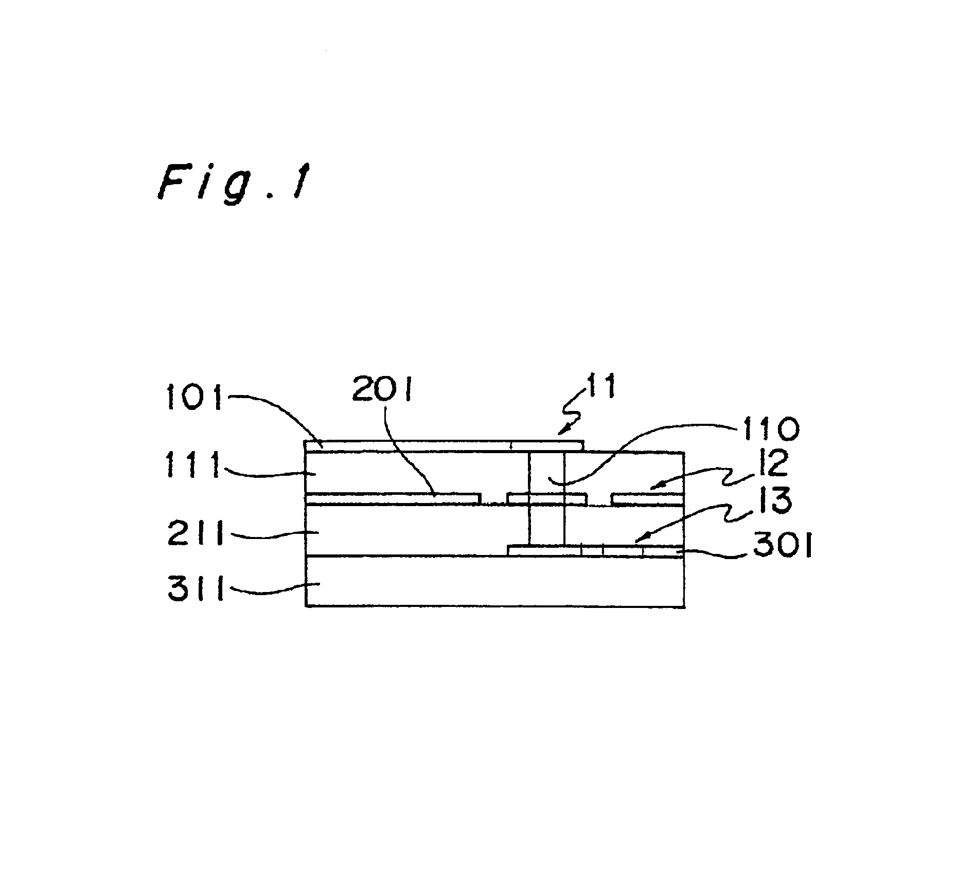
As is apparent from FIG. 10, low-reflection low-loss inter-circuit-layer transmission at a frequency of 60 GHz can be achieved with a simple structure employing the high-frequency multilayer circuit substrate of this

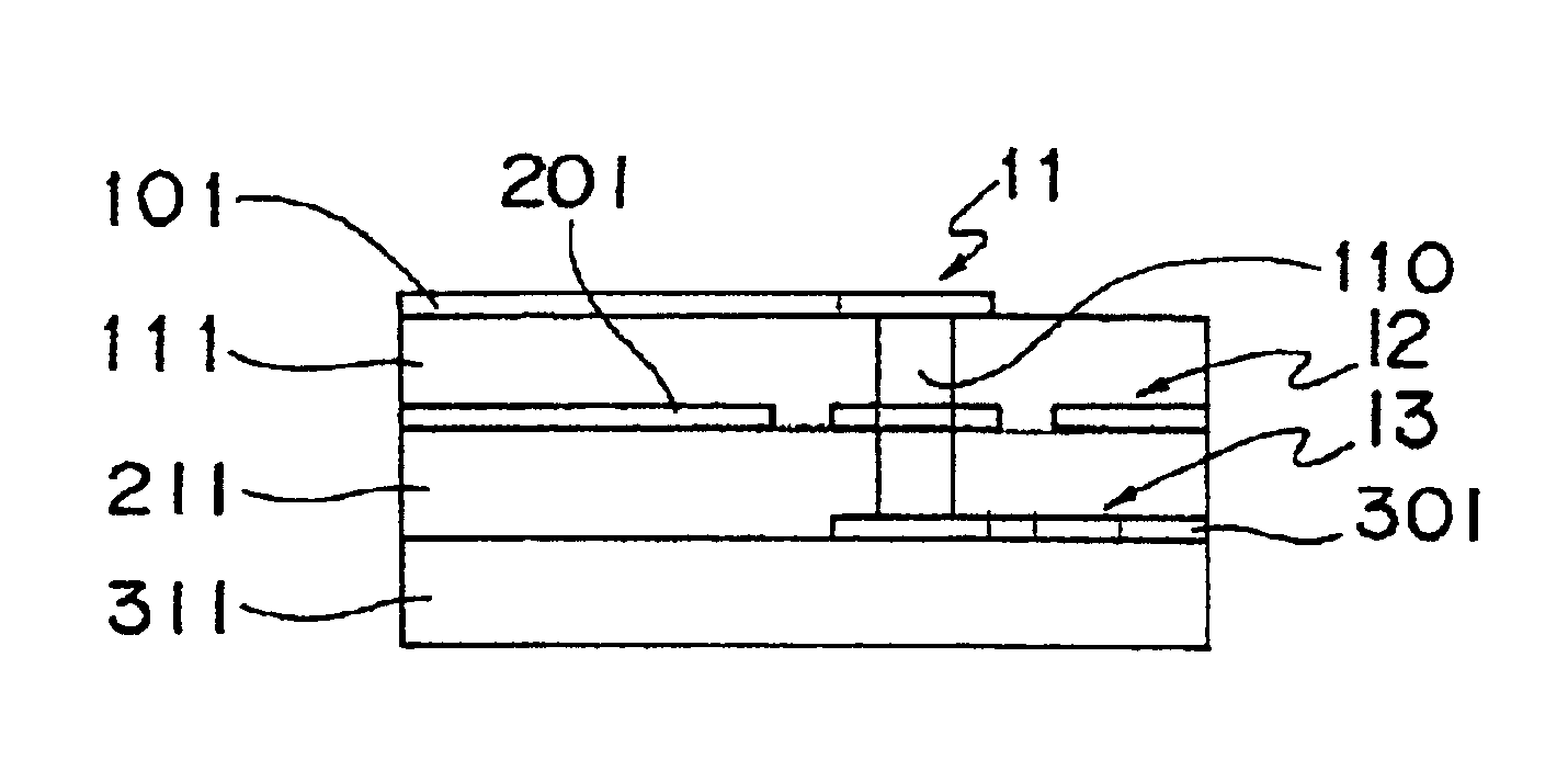
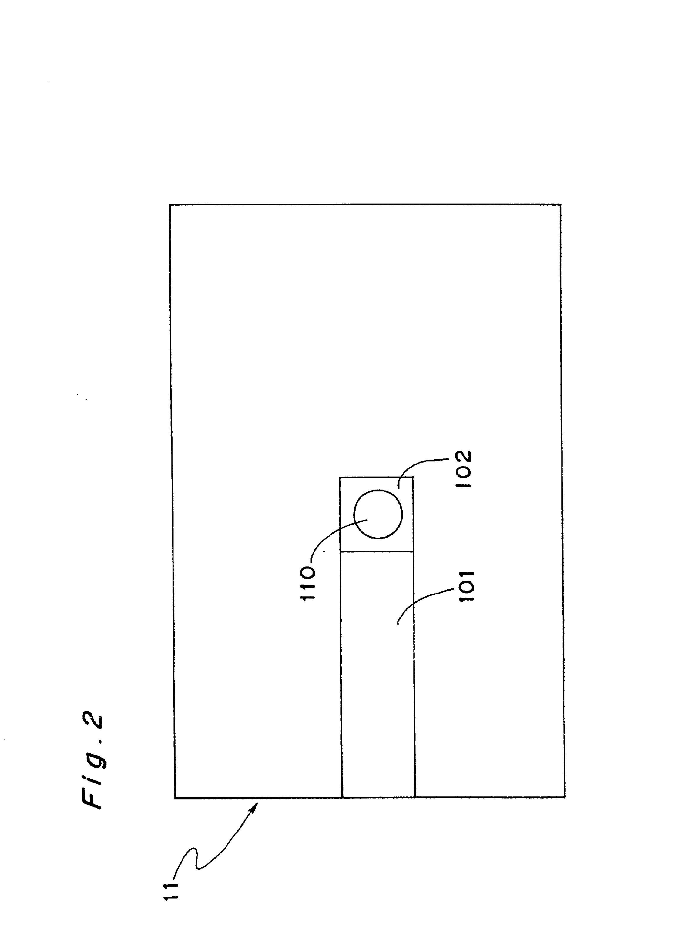
In the aforementioned first and second embodiments, the two signal transmission lines connected by way of the via hole are respectively arranged in the circuit layers located on both sides of the ground conductor layer. However, it is possible to arrange the two signal transmission lines connected by way of the via hole in the circuit layers located on an identical side with respect to the ground conductor layer.

Although the microstrip line is employed for the signal transmission line in the aforementioned first and second embodiments, the same effects can be obtained even when a coplanar line or a strip line is used.

Furthermore, in the aforementioned first and second embodiments, the characteristic impedance of the via hole connecting portion is matched to the character...


PUM


Abstract

A high-frequency multilayer circuit substrate having a plurality of circuit layers includes a via hole for connection between the circuit layers, a metal pad, an impedance matching transmission line, rectangular stubs and a signal transmission line. A via hole connecting portion is constructed of the via hole, the rectangular stubs and the impedance matching transmission line. A characteristic impedance of the via hole connecting portion is matched to a characteristic impedance of the signal transmission line by adjusting widths and lengths of the impedance matching transmission line and the rectangular stubs. Thereby, the reflection of the signal wave in the via hole connecting portion is reduced to decrease a transmission loss.

Description

BACKGROUND OF THE INVENTIONThe present invention relates to a high-frequency multilayer circuit substrate used in a microwave band and employing a via hole for connection between circuit layers.There has conventionally been a high-frequency multilayer circuit substrate, in which transmission lines are connected by way of a via hole provided for the improvement in performance of a high-frequency circuit and for high-density mounting. As reduction in size and increase in transmission signal frequency of this multilayer circuit substrate have been needed, a transmission loss due to signal wave reflection in the transmission lines and a via hole connecting portion has become a more serious trouble. In contrast to this, according to Japanese Patent Laid-Open Publication No. HEI 11-15037, characteristic impedance matching of the via hole connecting portion is achieved by providing a plate-shaped ground conductor of a specified width with a specified interval provided apart from a transmis...

Claims


Application Information

Patent Timeline
IPC IPC(8): H01P3/08H05K1/02H05K3/46
CPCH01P3/088H05K1/0251H05K2201/09781H05K2201/09727H05K2201/09718
Inventor ZHU, YUSUEMATSU, EIJI
Owner SHARP KK
Why Eureka
Try Eureka