Chip resistor

a chip resistor and resistor technology, applied in the field of chip resistors, can solve the problems of inability to enhance the rated value of the chip resistor, the cover coat is brought into contact or comes too close with the printed circuit board, and the chip resistor is often disadvantageously inclined, so as to achieve the effect of reducing manufacturing costs and reliably preventing the corrosion of the upper electrodes

Active Publication Date: 2005-02-15
ROHM CO LTD
View PDF13 Cites 29 Cited by
  • Summary
  • Abstract
  • Description
  • Claims
  • Application Information

AI Technical Summary

Benefits of technology

With such a feature, corrosion due to e.g. sulfur in the atmosphere does not occur at the auxiliary upper electrodes, whereby corrosion of the upper

Problems solved by technology

Therefore, when such a chip resistor is mounted on a printed circuit board with the resistor film facing the printed circuit board, the chip resistor is often disadvantageously inclined with one end thereof rising to be away from the circuit board.
However, in such a prior art chip resistor, the auxiliary upper electrodes do not project largely relative to the obverse surface of the cover coat.
Therefore, when the chip resistor is mounted on a printed circuit board with the resistor film facing the printed circuit board, the cover coat is brought into contact with or comes too close to the printed circuit board.
Since the printed wiring board in such a state is likely to be influenced by the heat generated at the heat re

Method used


Image

  • Chip resistor
  • Chip resistor
  • Chip resistor

Examples


Embodiment Construction

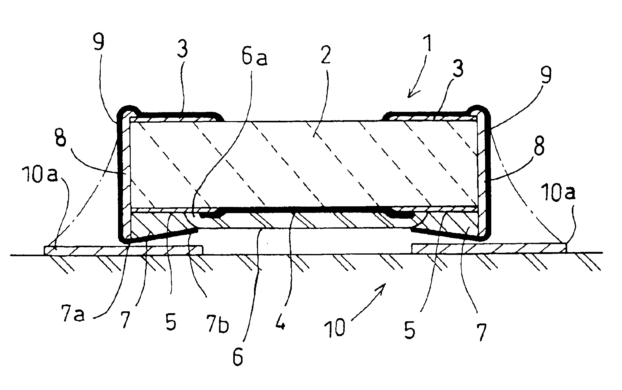
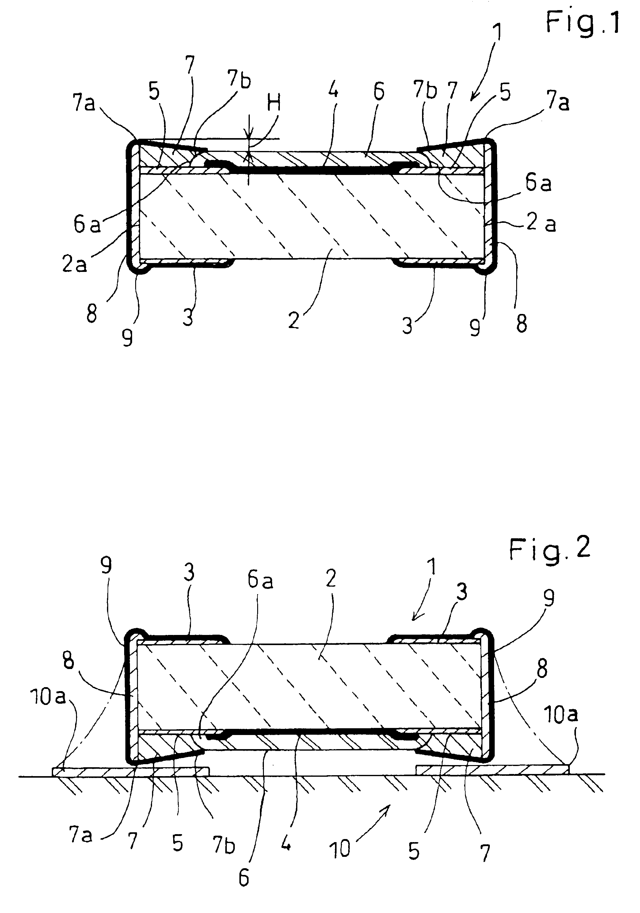
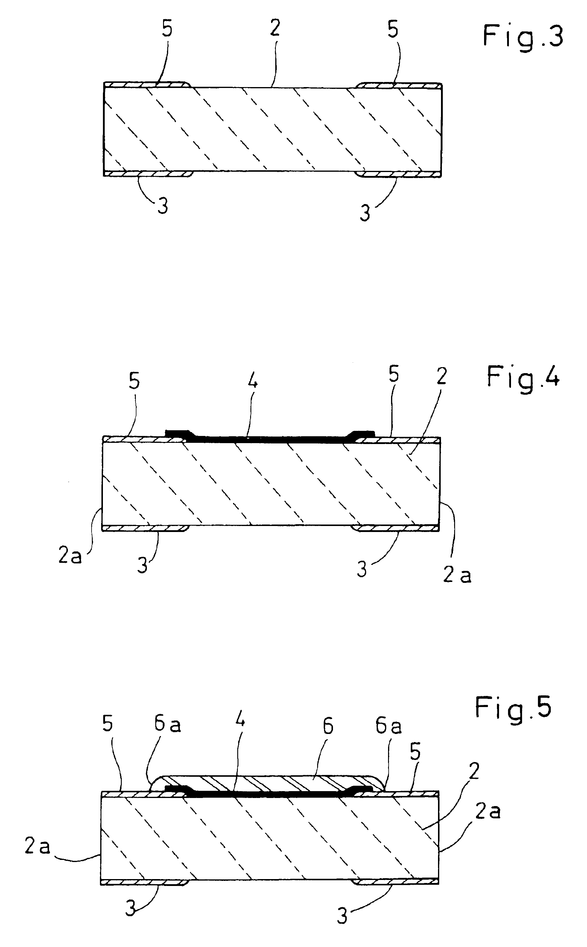
A chip resistor 1 according to an embodiment of the present invention includes an insulating substrate 2 in the form of a chip made of a heat-resistant material such as ceramic material. The insulating substrate 2 has a lower surface provided with a pair of lower electrodes 3 made of a conductive paste mainly composed of silver, which has a relatively low electric resistance. (Hereinafter, the paste is referred to as “silver-based conductive paste”.) The insulating substrate 2 has an upper surface formed with a resistor film 4, and a pair of upper electrodes 5 flanking and connected to the resistor film 4. The upper electrodes 5 are also made of a silver-based conductive paste. The chip resistor 1 further includes a cover coat 6 made of e.g. glass for covering the resistor film 4. The cover coat 6 overlaps part of each of the upper electrodes 5.

Each of the upper electrodes 5 has an upper surface formed with an auxiliary upper electrode 7 made of a silver-based conductive paste. The ...


PUM


Abstract

A chip resistor includes an insulating substrate 2 in the form of a chip having an upper surface and an opposite pair of side surfaces, a resistor film 4 formed on the upper surface of the insulating substrate 2, a pair of upper electrodes 5 formed on the upper surface of the insulating substrate 2 to flank the resistor film 4 in electrical connection thereto, a cover coat 6 covering the resistor film 4, an auxiliary upper electrode 7 formed on each of the upper electrodes 5 and including a first portion 7a adjoining the relevant side surface of the insulating substrate 2 and a second portion 7b overlapping the cover coat 6, and a side electrode 8 formed on each of the side surfaces of the insulating substrate 2 and electrically connected to at least the upper electrode 5 and the auxiliary upper electrode 7. The first portion 7a of the auxiliary upper electrode 7 has an obverse surface positioned higher than an obverse surface of the second portion 7b for projecting above an obverse surface of the cover coat 6.

Description

BACKGROUND OF THE INVENTION1. Field of the InventionThe present invention relates to a chip resistor comprising an insulating substrate in the form of a chip, at least one resistor film formed on the substrate, a pair of terminal electrodes formed on the substrate to flank the resistor film, and a cover coat covering the resistor film.2. Description of the Related ArtConventionally, in a chip resistor of the above-described type, the cover coat covering the resistor film projects largely from a central portion of the upper surface of the insulating substrate, thereby providing stepped portions in the chip resistor. Therefore, when such a chip resistor is mounted on a printed circuit board with the resistor film facing the printed circuit board, the chip resistor is often disadvantageously inclined with one end thereof rising to be away from the circuit board.JP-A-8-236302 discloses a chip resistor capable of solving such a problem. Specifically, as shown in FIG. 9 of JP-A-8-236302, ...

Claims


Application Information

Patent Timeline
IPC IPC(8): H01C17/00H01C17/28H01C7/00H01C1/14H01C1/142
CPCH01C1/142H01C17/281H01C17/006H01C7/003
Inventor KURIYAMA, TAKAHIRODOI, MASATO
Owner ROHM CO LTD
Why Eureka
Try Eureka