Apparatus for and method of manufacturing a semiconductor die carrier

a technology of die carrier and semiconductor, which is applied in the direction of metal working apparatus, other manufacturing equipment/tools, manufacturing tools, etc., can solve the problems of increasing repetitive manufacturing process, high risk of bending or damaging leads either before or during insertion into both the bandolier or the package, and achieves the effect of easy insertion of a varying number of leads into the substra

Inactive Publication Date: 2005-02-22
IQLP
View PDF92 Cites 9 Cited by
  • Summary
  • Abstract
  • Description
  • Claims
  • Application Information

AI Technical Summary

Benefits of technology

A further object of the invention is to provide an apparatus for inserting conductive leads that utilizes feedback from photographic, optical, and electronic signals to accurately insert leads into a substrate.
A further object of the invention is to provide an apparatus for inserting conductive leads that includes multiple lead supplies and multiple substrate supplies to permit the apparatus to run operations in parallel and eliminate down time with minimal operator supervision.
A further object of the invention is to provide an apparatus that can easily insert a varying number of leads into a substrate.
A further object of the invention is to provide a method of economically manufacturing an electrical component with external leads, such as a semiconductor die carrier.

Problems solved by technology

As more conductive leads are required for each semiconductor die carrier, the manufacturing process becomes increasingly repetitive and time consuming.
Further, conventional machines are limited in their adjustability regarding the depth of lead insertion and the spacing between leads along the side walls of the package.
In a bandolier system, the risk of bending or damaging leads either before or during insertion into both the bandolier or the package is very high.
Obviously, this method takes an inordinate amount of time and the leads may be damaged during handling or insertion.

Method used


Image

  • Apparatus for and method of manufacturing a semiconductor die carrier
  • Apparatus for and method of manufacturing a semiconductor die carrier
  • Apparatus for and method of manufacturing a semiconductor die carrier

Examples


Embodiment Construction

Reference will now be made in detail to the present exemplary embodiment(s) of the invention illustrated in the accompanying drawings. Wherever possible, the same reference numbers will be used throughout the drawings to refer to the same or like parts.

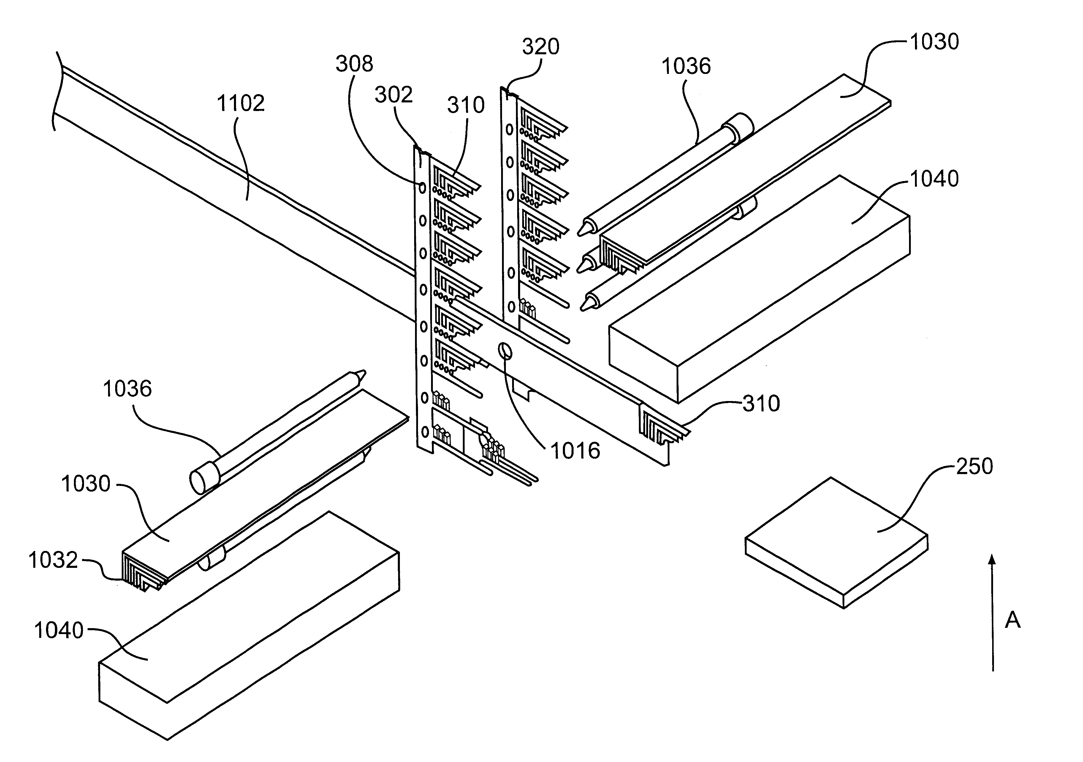
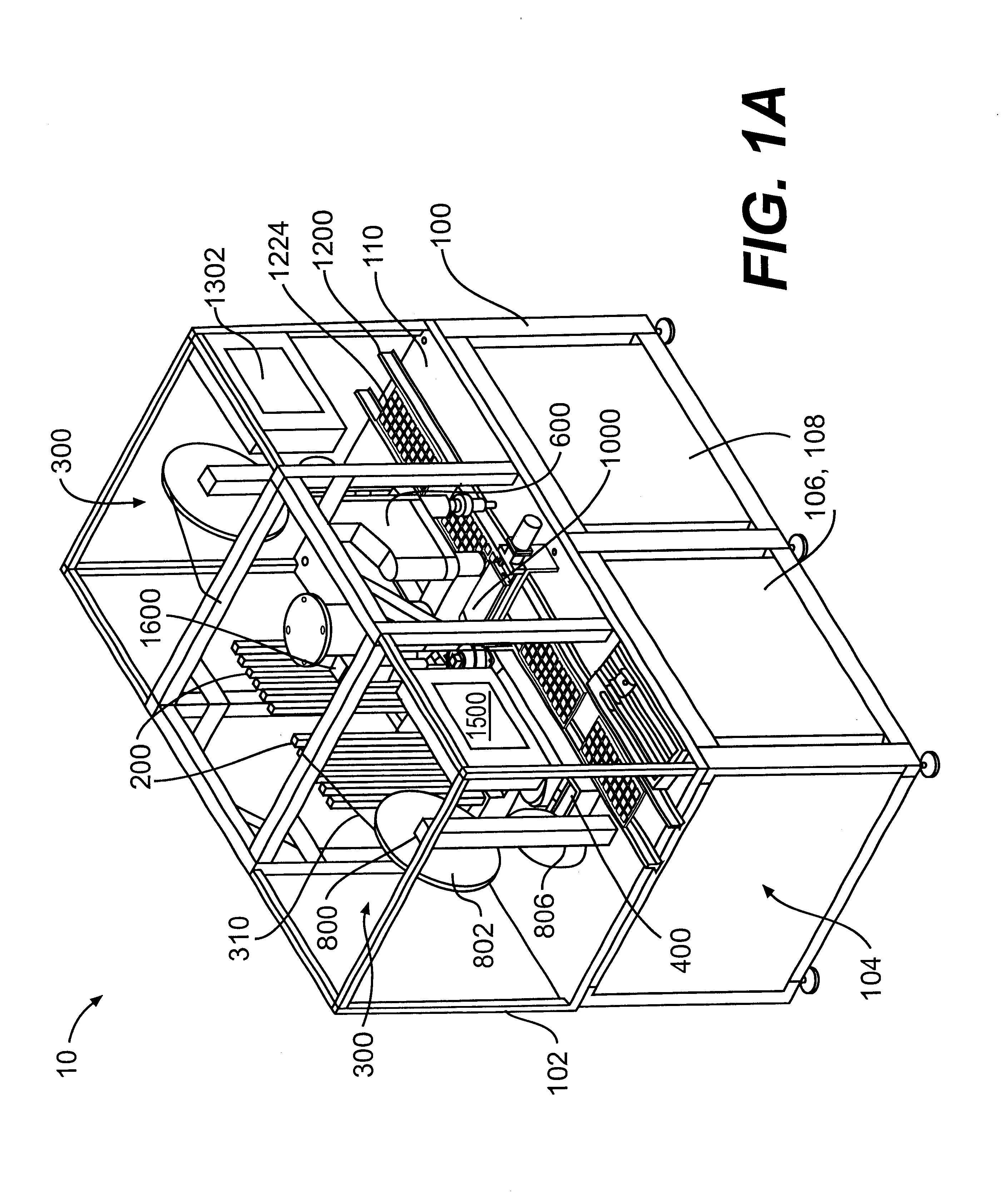
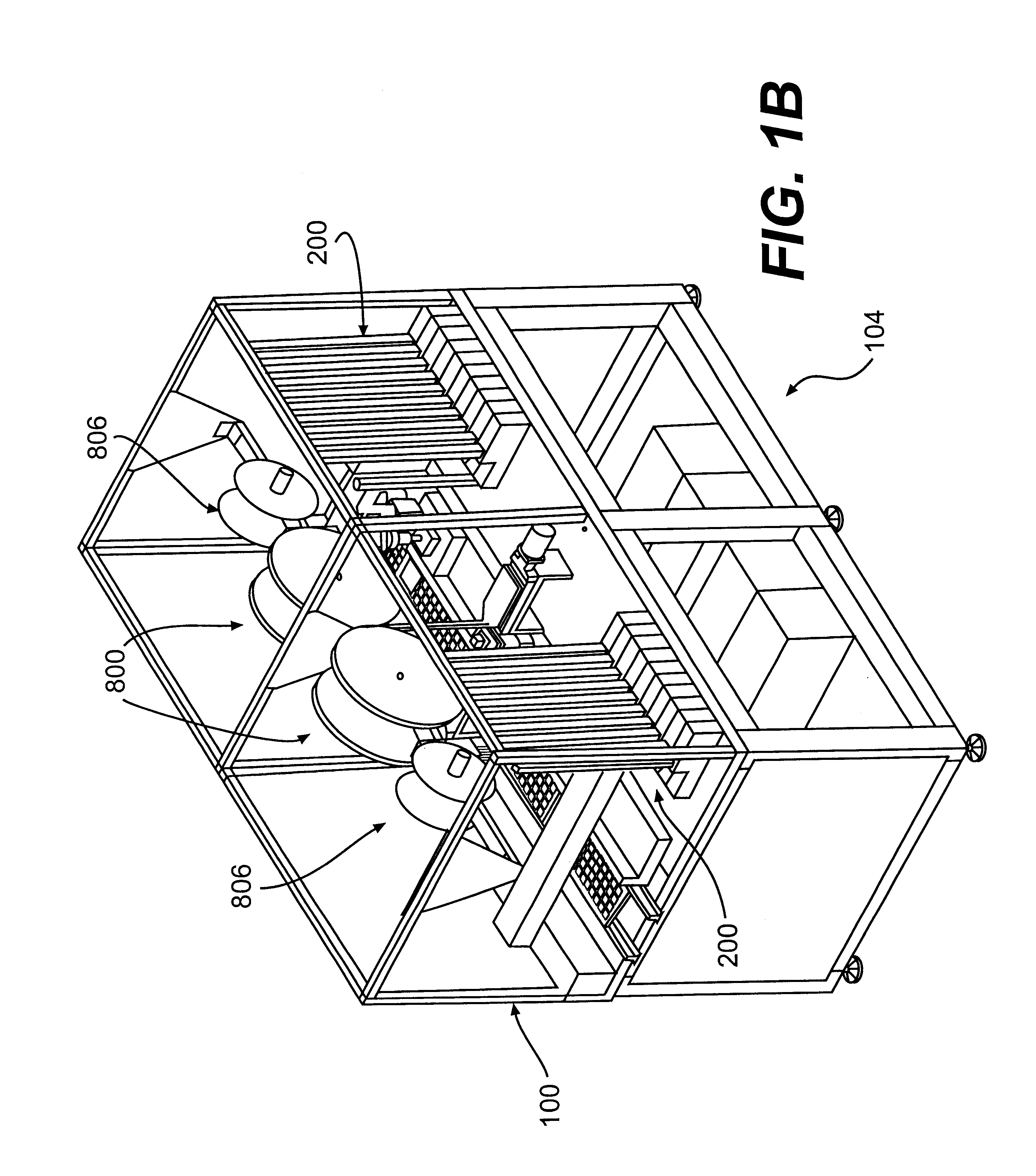
The apparatus in accordance with an embodiment of the invention includes a first feed mechanism for feeding multiple supply lines of conductive leads to the apparatus, each of the supply lines comprising a plurality of conductive leads mounted on a transport medium, and a second feed mechanism for feeding individual substrates to the apparatus for conductive lead insertion. The apparatus further includes a mandrel for holding an individual substrate during the insertion of the leads, a product carriage for receiving the substrates after insertion of the leads, and a conductive lead insertion mechanism. The lead insertion mechanism receives conductive leads from the first feed mechanism, and the lead insertion mechanism is adapted to s...


PUM

PropertyMeasurementUnit
conductiveaaaaaaaaaa
timeaaaaaaaaaa
insertion depthaaaaaaaaaa

Abstract

A lead insertion machine includes a substrate supply, a conductive lead supply, and an lead insertion mechanism. The conductive leads are inserted into lead passages formed in side walls of the substrate. Also disclosed is a method of manufacturing a semiconductor die carrier including the steps of forming a plurality of conductive leads, forming a substrate for holding a semiconductor die, the substrate having a plurality of insulative side walls defining an exterior surface of the substrate, each of the side walls having a plurality of lead passages formed therethrough, and simultaneously inserting at least one of the conductive leads into the lead passage of one of the side walls for retention therein and at least one other of the conductive leads into the lead passage of another of the side walls for retention therein.

Description

BACKGROUND OF THE INVENTION1. Field of the InventionThe present invention relates to an apparatus and method for manufacturing an electrical component and, more particularly, a semiconductor die carrier, and to an apparatus and method for inserting conductive leads into side walls of a substrate that holds a semiconductor die.2. Description of the Prior ArtSemiconductor dies have numerous applications in the world today. The dies are usually supported in a housing or carrier (also known as a “package”) that protects the die and facilitates the connection of the die to a substrate or a board, depending on the application. The carriers often include conductive leads that establish an electrical connection between the semiconductor die and a substrate or board.Semiconductor die carriers are typically manufactured by molding a plastic housing around a lead frame. The lead frame connects individual leads to maintain their position during molding.The assignee has adopted a different appro...

Claims


Application Information

Patent Timeline
Patent Type & Authority Patents(United States)
IPC IPC(8): H01L21/00H01L23/12
CPCH01L21/67121H01L2924/0002Y10T29/53261Y10T29/49139Y10T29/5142Y10T29/53183Y10T29/49147Y10T29/5193H01L2924/00H01L21/50
Inventor CRANE, JR., STANFORD W.LARCOMB, DANIELKRISHNAPURA, LAKSHMINARASIMHA
Owner IQLP
Why Eureka
Try Eureka