Channel-etch thin film transistor
- Summary
- Abstract
- Description
- Claims
- Application Information
AI Technical Summary
Benefits of technology
Problems solved by technology
Method used
Image

Examples
first embodiment
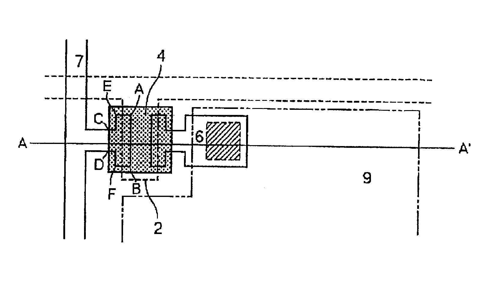
A first embodiment according to the present invention will be described in detail with reference to the drawings. FIG. 6 is a fragmentary plan view of a novel channel-etch thin film transistor with improved source and drain electrodes in accordance with a first embodiment of the present invention. FIG. 7 is a fragmentary cross sectional elevation view taken along an A-A′ line of FIG. 6. With reference to FIGS. 6 and 7, a structure of the novel channel-etch thin film transistor will, hereinafter, be described.
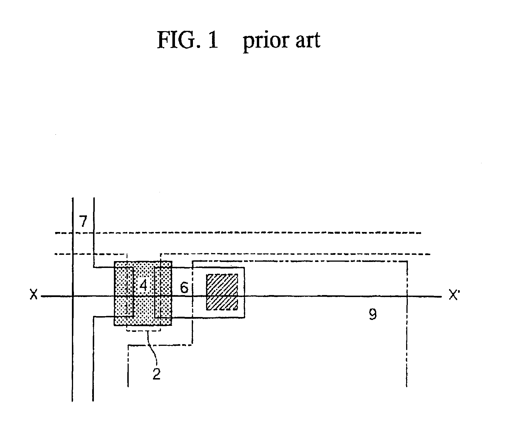
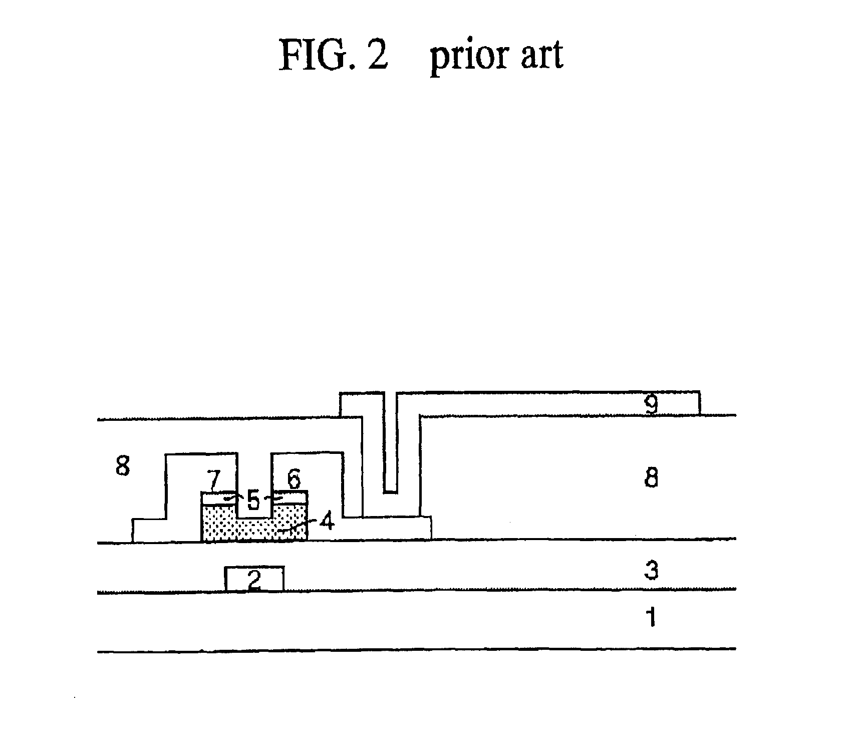
In summary, a structural difference between the novel channel-etch thin film transistor shown in FIGS. 6 and 7 in this first embodiment of the present invention and the conventional channel-etch thin film transistor shown in FIGS. 1 and 2 appears only on the plan shapes of the source and drain electrodes. Namely, there is no structural difference in the cross sectional elevation view in FIGS. 2 and 7.
In details, a gate electrode 2 of chromium (Cr) is selectively provided on an u...
second embodiment
A second embodiment of the present invention will be described. FIG. 12 is a fragmentary plan view of a novel channel-etch thin film transistor with improved source and drain electrodes in accordance with a second embodiment of the present invention. FIG. 13 is a fragmentary cross sectional elevation view taken along a B-B′ line of FIG. 12. With reference to FIGS. 12 and 13, a structure of the novel channel-etch thin film transistor will, hereinafter, be described.
In summary, a structural difference between the novel channel-etch thin film transistor shown in FIGS. 12 and 13 in this first embodiment of the present invention and the conventional channel-etch thin film transistor shown in FIGS. 1 and 2 appears on both the plan view and the cross sectional view of the source and drain electrodes. Each of the source and drain electrodes 6 and 7 extends in contact with the top surface of the active layer 4 but separated from the side walls of the active layer 4 by the inter-layer insulat...
PUM
 Abstract
Description
Claims
Application Information