Package structure of organic electroluminescence panel

a technology of organic electroluminescence and packaging structure, which is applied in the direction of circuit arrangement on insulating boards, semiconductor devices, electrical apparatus, etc., can solve the problems of oel device a little late, common-use substrate warpage, and still encountering size restrictions, etc., to achieve low stress force, less problem, and better conductivity

Inactive Publication Date: 2005-02-22
III HLDG 1
View PDF3 Cites 6 Cited by
  • Summary
  • Abstract
  • Description
  • Claims
  • Application Information

AI Technical Summary

Benefits of technology

An objective of the present invention is to provide a packaging structure for the OEL panel with less issue on low stress force and better conductivity.
Another objective of the present invention is to provide a packaging structure for the OEL panel, in which multiple OEL panels can be assembled to the same printed circuit board, so as to breakthrough the restriction of size for the huge size.
In accordance with the foregoing and other objectives of the present invention, the invention provides a package structure of the OEL panel, including a printed circuit board, one or multiple OEL panels, multiple bumps, and underfill. Wherein, the printed circuit board has multiple solder pads, and at least one OEL panel is implemented on the printed circuit board. The bumps are respectively disposed between the solder pads on the printed circuit board and the poly solder interconnections, so as to have the electric connection for the OEL panel and the printed circuit board. In addition, the underfill is disposed between the printed circuit board and the panel. The underfill includes, for example, the hydrophobic material, having the ability of preventing the water from diffusing in and the stress buffer at the same time.

Problems solved by technology

However, comparing with the other display technology, the development for OEL device is a little late, the technology has not been completely developed yet.
Even though the packaging structure for the foregoing OEL panel can effectively integrate the driving chip onto the same substrate, it still encounters a restriction of size when a larger size is eventually desired.
Even though the foregoing packaging structure for the OEL panel can use several display blocks for assembly, so as to achieve the objective of huge size, during soldering the contact pads and the bumps, the necessary high temperature in the solder reflowing process would often cause the common-use substrate to be warped.
Moreover, the high temperature solder reflowing process would also cause improper affection on the organic light emitting layer in the OEL panel.

Method used


Image

  • Package structure of organic electroluminescence panel
  • Package structure of organic electroluminescence panel
  • Package structure of organic electroluminescence panel

Examples


first embodiment

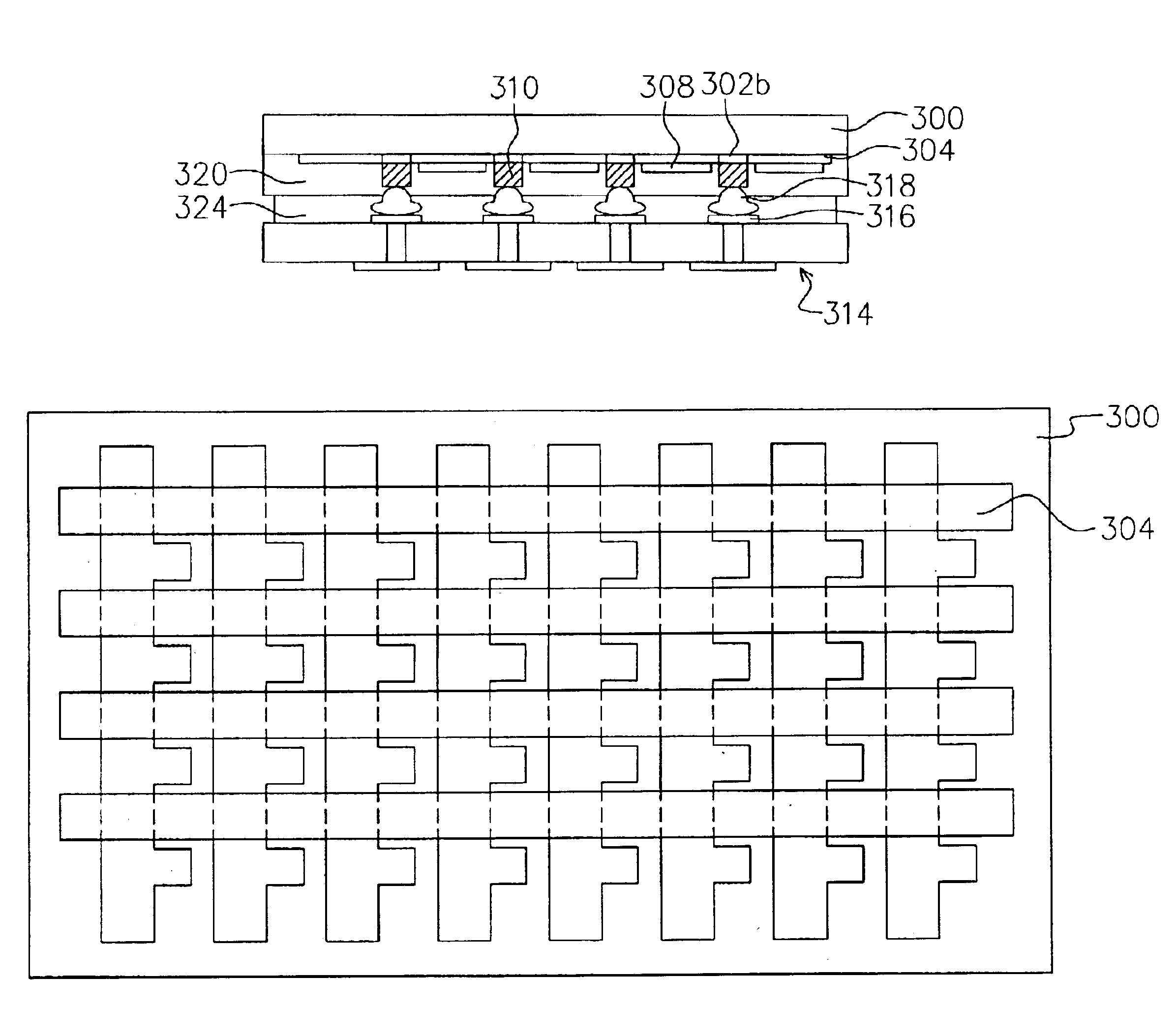
Embodiment 1: FIGS. 3-6, are drawings, schematically illustrating the process to fabricate an OEL panel, according to the present invention. In FIG. 3, a transparent substrate 300 is provided. Th transparent substrate 300 includes, for example, glass, acrylate, or other transparent materials. The transparent substrate 300 is formed with several anodes 302. The anode 302 includes a driving region 302a and at least one contact region 302b. The anode 302 includes the material, such as indium tin oxide (ITO) or other transparent conductive material. Wherein, the driving region 302a has, for example, a stripe pattern and parallel to each other, on the transparent substrate 300. The contact region 302b is protruding out from the driving region 302a, and is used for external connection to the other region.

Referring to FIG. 4, after the anodes 302 have been formed, a patterned organic light emitting layer 304 is formed on the transparent substrate 300. The patterned organic light emitting l...

second embodiment

Embodiment 2: FIGS. 9-12 are drawings, schematically illustrating the process to fabricate an OEL panel, according to the present invention. First, referring to FIG. 9, a transparent substrate 300 is provided. The transparent substrate 300 includes, for example, glass, acrylate, or other transparent materials. The transparent substrate 300 is formed with several anodes 302. The anode 302 includes a driving region 302a and at least one contact region 302b. The anode 302 includes the material, such as indium tin oxide (ITO) or other transparent conductive material. Wherein, the driving region 302a has, for example, a stripe pattern and parallel to each other, on the transparent substrate 300. The contact region 302b is protruding out from the driving region 302a, and is used for external connection to the other region.

Referring to FIG. 10, after the anodes 302 have been formed, a patterned organic light emitting layer 304 is formed on the transparent substrate 300. The patterned organ...


PUM


Abstract

A package structure of an OEL panel includes a printed circuit board, at least one OEL panel, and several bumps. Wherein, the OEL panel has several poly solder interconnections arranged in an array structure. The printed circuit board has several solder pads, which are also implemented with bumps. The at least one OEL panel is disposed on the printed circuit board to have the electric connection with the printed circuit board through the poly solder interconnections and the bumps.

Description

CROSS REFERENCE TO RELATED APPLICATIONSThis application claims the priority benefit of Taiwan application serial no.91201632, filed on Feb. 8, 2002.BACKGROUND OF INVENTION1. Field of InventionThe present invention relates to a package structure of an organic electroluminescence (OEL) panel. More particularly, the present invention relates to a package structure of an OEL panel, having the poly solder interconnection arranged in an array structure.2. Description of Related ArtThe OEL device is a device that uses the organic functional materials with the property of spontaneous light-emitting to achieve the displaying effect. According to the different molecular weight of the organic functional materials, it can be categorized into a small molecular organic light emitting device (SM-OLED) and the polymer light-emitting device (PLED).The OEL device is using two electrodes to hold an organic functional material film from both sides. When a proper bias is applied on it, the holes will be...

Claims


Application Information

Patent Timeline
Patent Type & Authority Patents(United States)
IPC IPC(8): H01L27/15H01L33/00H05K7/02H05K7/06H01L27/32
CPCH01L27/3288H01L51/529H01L27/3293H10K59/179H10K59/18H10K50/87
Inventor WU, CHIN-LONGTANG, TUNG-YANGHSU, SHIH-MINGCHEN, SHANG-WEIHUANG, TEIN-WANG
Owner III HLDG 1
Why Eureka
Try Eureka