Packaged semiconductor device and method of formation
- Summary
- Abstract
- Description
- Claims
- Application Information
AI Technical Summary
Problems solved by technology
Method used
Image

Examples
Embodiment Construction
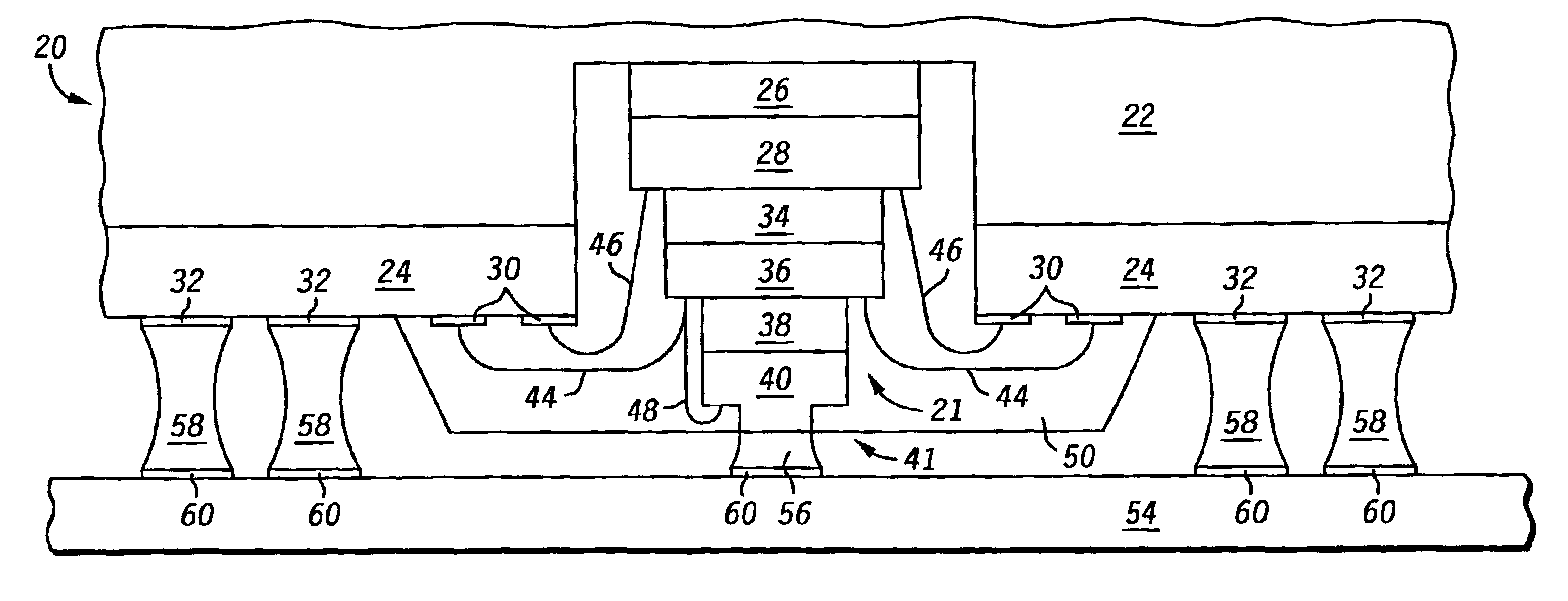
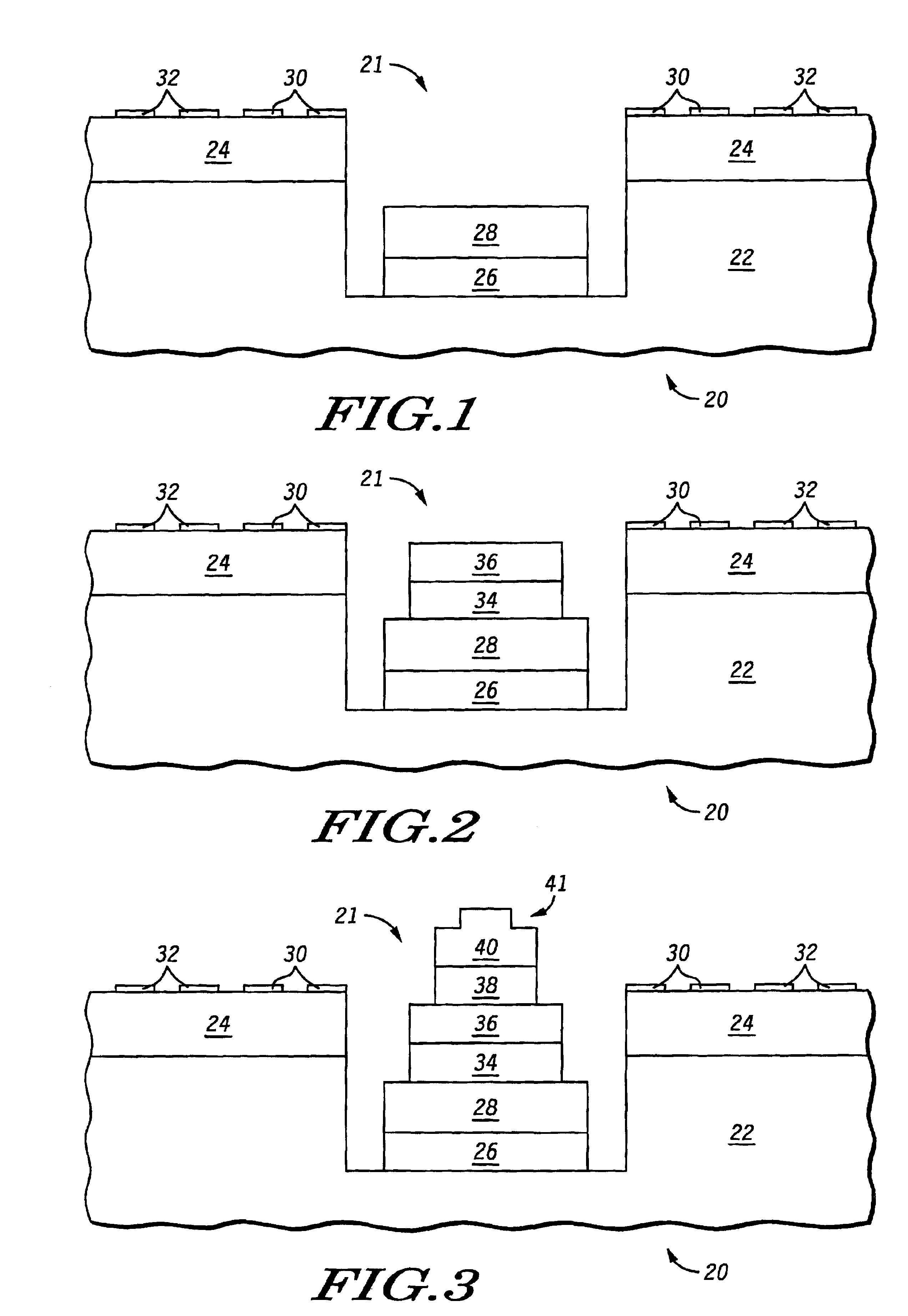
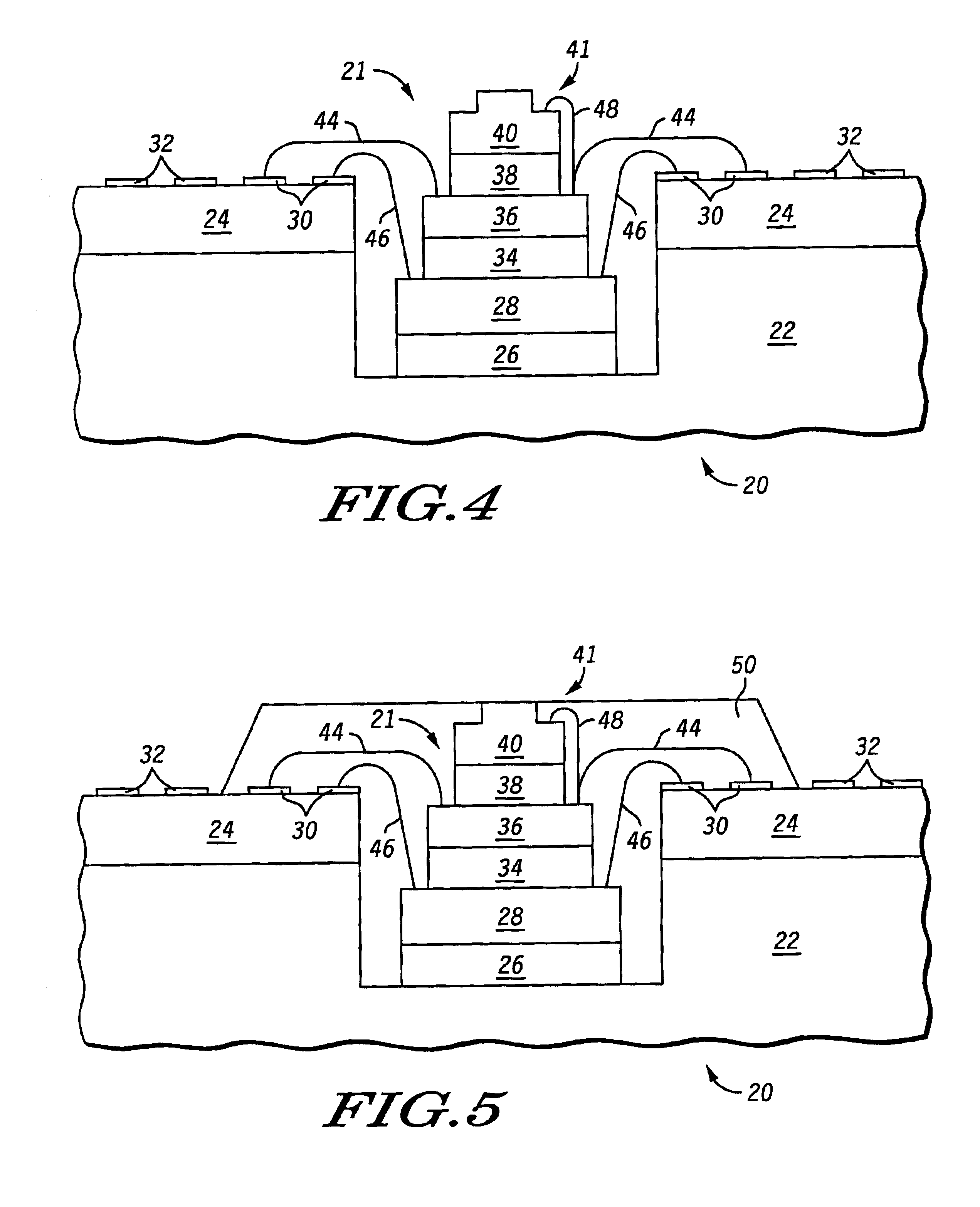
Generally, the present invention provides a packaged semiconductor device for stacked die that improves thermal dissipation by attaching a heat spreader to the top die. The heat spreader attached to the top die supplements a heat spreader that is used to support the bottom die. The bottom heat spreader has a cavity for supporting the stacked die to reduce the height of the device. When the packaged device is attached to a printed circuit board (PCB), the heat spreader attached to the top die contacts the PCB and provides a direct thermal path for sinking heat generated by the operation of the top die. The invention is better understood by turning to the figures.
FIG. 1 illustrates a device 20 in accordance with an embodiment of the present invention. Packaged device 20 includes a heat spreader 22 having a cavity 21. In the illustrated embodiment, heat spreader 22 is formed from copper. If formed from copper, heat spreader 22 may be plated with another metal such as chromium silver, n...
PUM
 Abstract
Description
Claims
Application Information
 - R&D Engineer
- R&D Manager
- IP Professional
- Industry Leading Data Capabilities
- Powerful AI technology
- Patent DNA Extraction
Browse by: Latest US Patents, China's latest patents, Technical Efficacy Thesaurus, Application Domain, Technology Topic.
© 2024 PatSnap. All rights reserved.Legal|Privacy policy|Modern Slavery Act Transparency Statement|Sitemap