Multi-concentric pad arrangements for integrated circuit pads

a technology of integrated circuit pads and concentrations, which is applied in the direction of electrical equipment, semiconductor devices, semiconductor/solid-state device details, etc., can solve the problems of limiting the number of pads on a die, the difficulty of reducing the i/o pad pitch of the ic die below approximately 50-100 microns, and the cost of the die is higher. achieve linear cost increase per pad count, increase the density of pads, and increase the effect of pad density

Inactive Publication Date: 2005-02-22
AVAGO TECH INT SALES PTE LTD
View PDF5 Cites 23 Cited by
  • Summary
  • Abstract
  • Description
  • Claims
  • Application Information

AI Technical Summary

Benefits of technology

By stacking the IO pads, a higher pad density is achieved with a linear cost increase per pad count. Thus, the present invention enables higher pad density using conventional packaging. In some embodiments, flip-chip redistribution layers are used, but this is not required of other embodiments of the present invention.

Problems solved by technology

In these methods, the physical limitations in wire bonding have made it difficult to reduce the I / O pad pitch of the IC die below approximately 50-100 microns.
This means that the die cost is higher.
There are numerous obstacles that limit the number of pads on a die.
The physical and geometrical structure of the pad itself is a major limiting factor.

Method used


Image

  • Multi-concentric pad arrangements for integrated circuit pads
  • Multi-concentric pad arrangements for integrated circuit pads
  • Multi-concentric pad arrangements for integrated circuit pads

Examples


Embodiment Construction

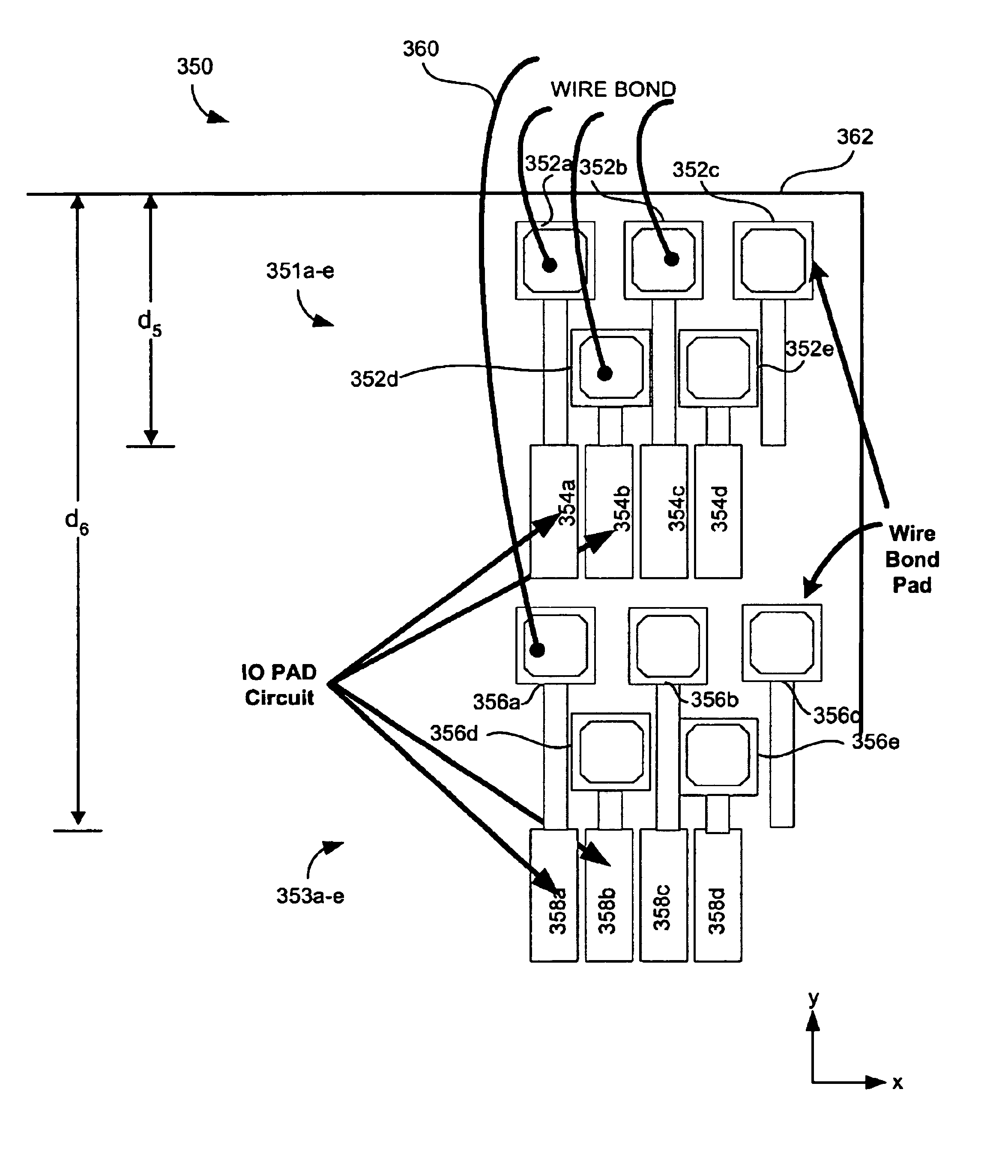
As introduced above, the present invention involves an approach to layering sets of MCP to increase pad density. FIGS. 3A-B, 4, and 5, described below, illustrate this approach with the use of pad sets and a mesh interconnect.

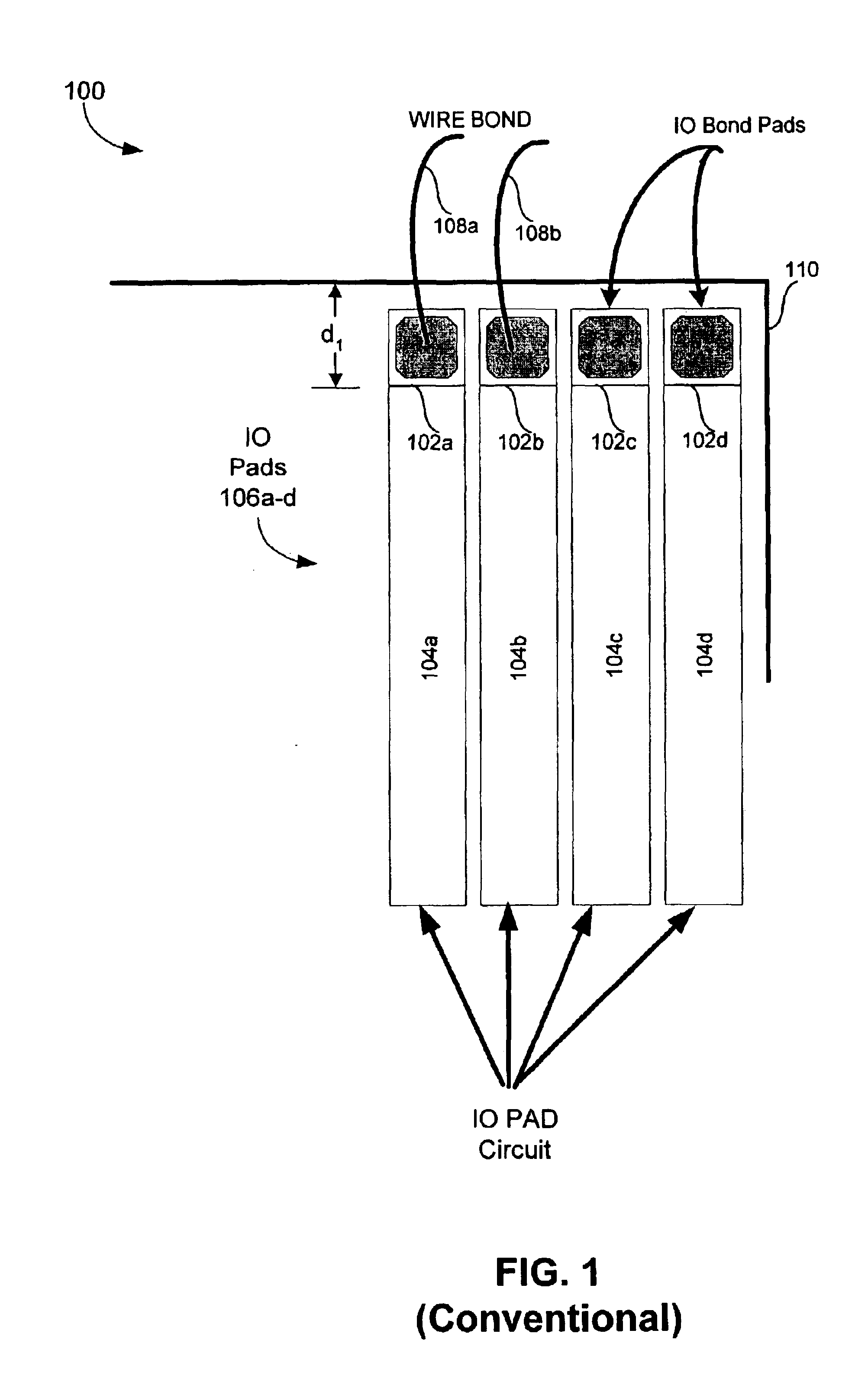
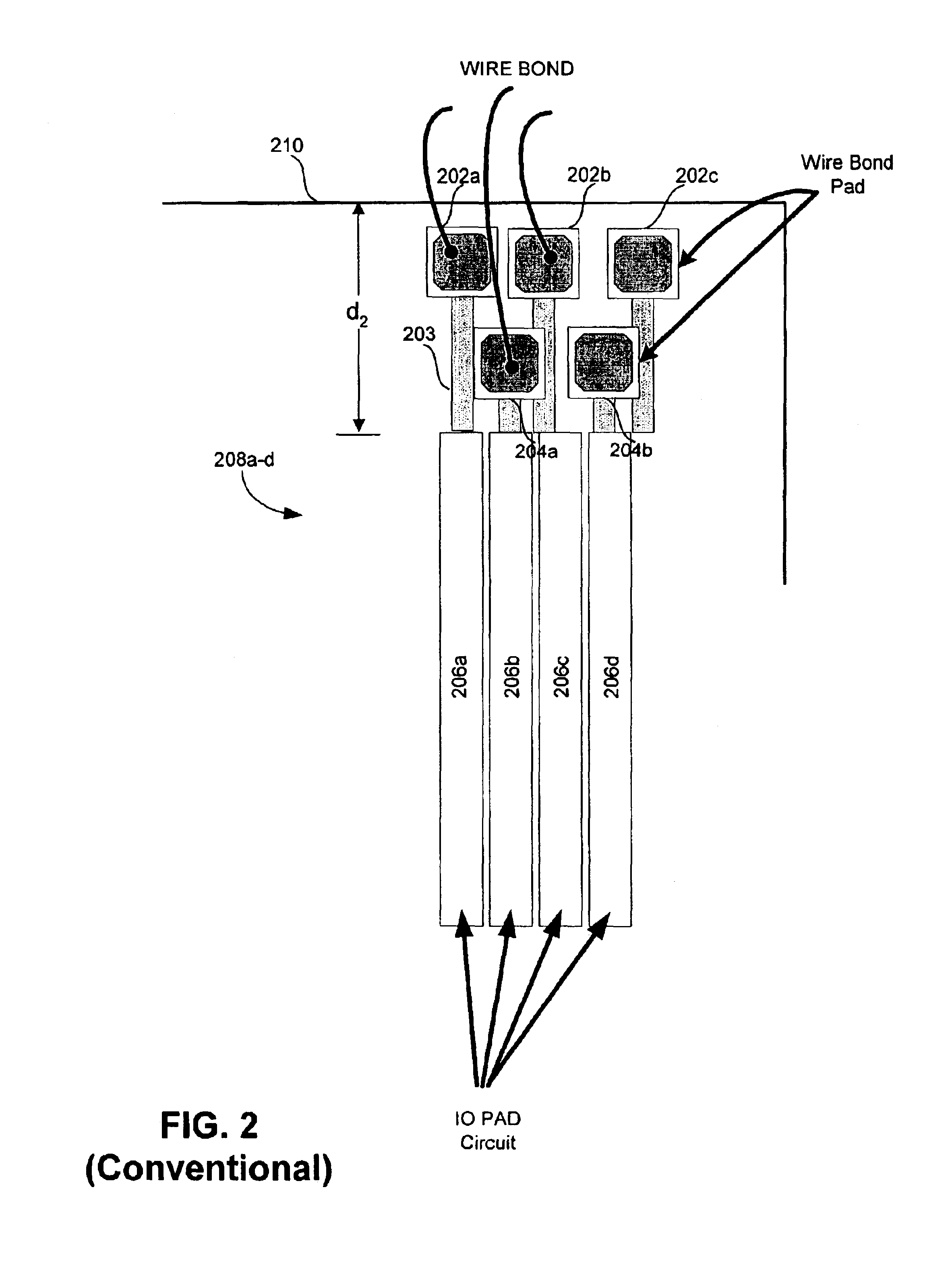
FIG. 3A shows an IC die 300 having a multi-concentric pad (MCP) arrangement based on an in-line pad arrangement according to an embodiment of the present invention. IC die 300 includes IO pad set (or row) 301 and IO pad set 303.

IO pad set 301 includes IO pads 301a, 301b, 301c, and 301d. Each IO pad 301 includes a bond pad 302 that is connected to an IO circuit 306. Bond wires 310 are bonded to the bond pads 302 in order to communicate input and output signals to and from the IC die 300. The IO pad circuits 306 provide any necessary interface circuitry between the IC die 300 and the external circuits connected to the bond pads 302. More specifically, the IO pad circuits 306 provide an interface to the core circuitry of the IC die 300.

Similarly, IO pad set 303 in...


PUM


Abstract

Multi-concentric pad (MCP) arrangements provide for increased pad densities on integrated circuits. The multi-concentric pad (MCP) configuration includes a first set of input output (IO) pads and a second set of IO pads, both disposed on an integrated circuit die. Each IO pad in said first set and said second set of IO pads includes a bond pad for receiving a bond wire connection, and an IO circuit coupled to the bond pad. The IO circuits provide an interface between a signal received at the corresponding bond pad and a core circuit disposed on said IC die. The first set of IO pads are arranged closer to the perimeter of the IC die than the second set of IO pads. Furthermore, the second set of IO pads are arranged so that each IO circuit in the second set of IO pads is closer to the center of the IC die than a corresponding IO circuit in the first set of IO pads.

Description

BACKGROUND OF THE INVENTION1. Field of the InventionThis invention relates generally to packages for integrated circuit devices, and placing input and output pads on an integrated circuit device in order to optimize the die size of the integrated circuit device.2. Related ArtThere are various methods for the wire bonding of packages which house integrated circuit (IC) dies. In these methods, the physical limitations in wire bonding have made it difficult to reduce the I / O pad pitch of the IC die below approximately 50-100 microns. In many high density I / O IC designs, this leads to die sizes that are considerably larger than the active core size. An integrated circuit die where the die size is larger than the active core size is referred to as “pad-limited.” Because a pad-limited die contains significant portions of the unused space, the die is larger and fewer dies will be printed per wafer. This means that the die cost is higher.There are numerous obstacles that limit the number of...

Claims


Application Information

Patent Timeline
Patent Type & Authority Patents(United States)
IPC IPC(8): H01L23/50H01L23/485H01L23/48
CPCH01L23/50H01L24/06H01L24/48H01L24/49H01L24/05H01L2224/05554H01L2224/04042H01L2224/05556H01L2224/05599H01L2224/48091H01L2224/4813H01L2224/48463H01L2224/49174H01L2224/49431H01L2224/85399H01L2924/01005H01L2924/01006H01L2924/01033H01L2924/01077H01L2924/14H01L2924/01068H01L2924/00014H01L2224/45099H01L2224/023H01L2924/0001
Inventor RAKSHANI, VAFA JAMES
Owner AVAGO TECH INT SALES PTE LTD
Why Eureka
Try Eureka