

Semiconductor die with high density offset-inline bond arrangement
a technology of offset inline bonding and semiconductor die, which is applied in the direction of semiconductor/solid-state device testing/measurement, semiconductor device details, semiconductor/solid-state device testing/measurement, etc., can solve the problems of inflexible technology, staggered bonding pads consuming a substantial portion of the available die area, so as to achieve the maximum bonding distance, the effect of increasing the density of the pad and increasing the bonding distan
- Summary
- Abstract
- Description
- Claims
- Application Information
AI Technical Summary
Benefits of technology
Problems solved by technology
Method used
Image

Examples
Embodiment Construction
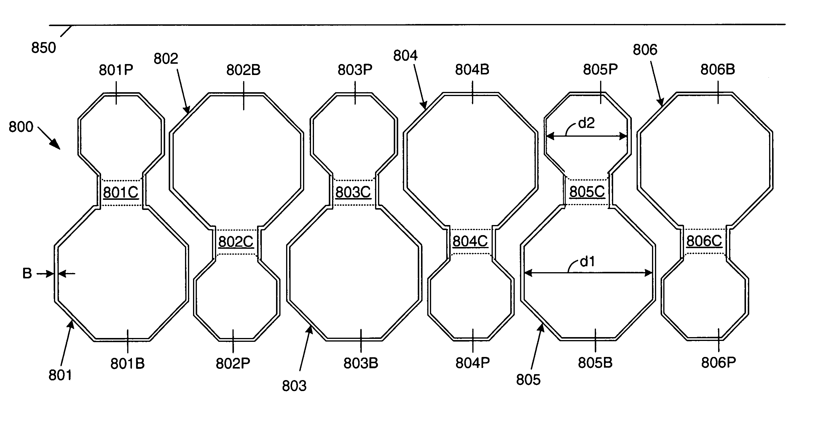
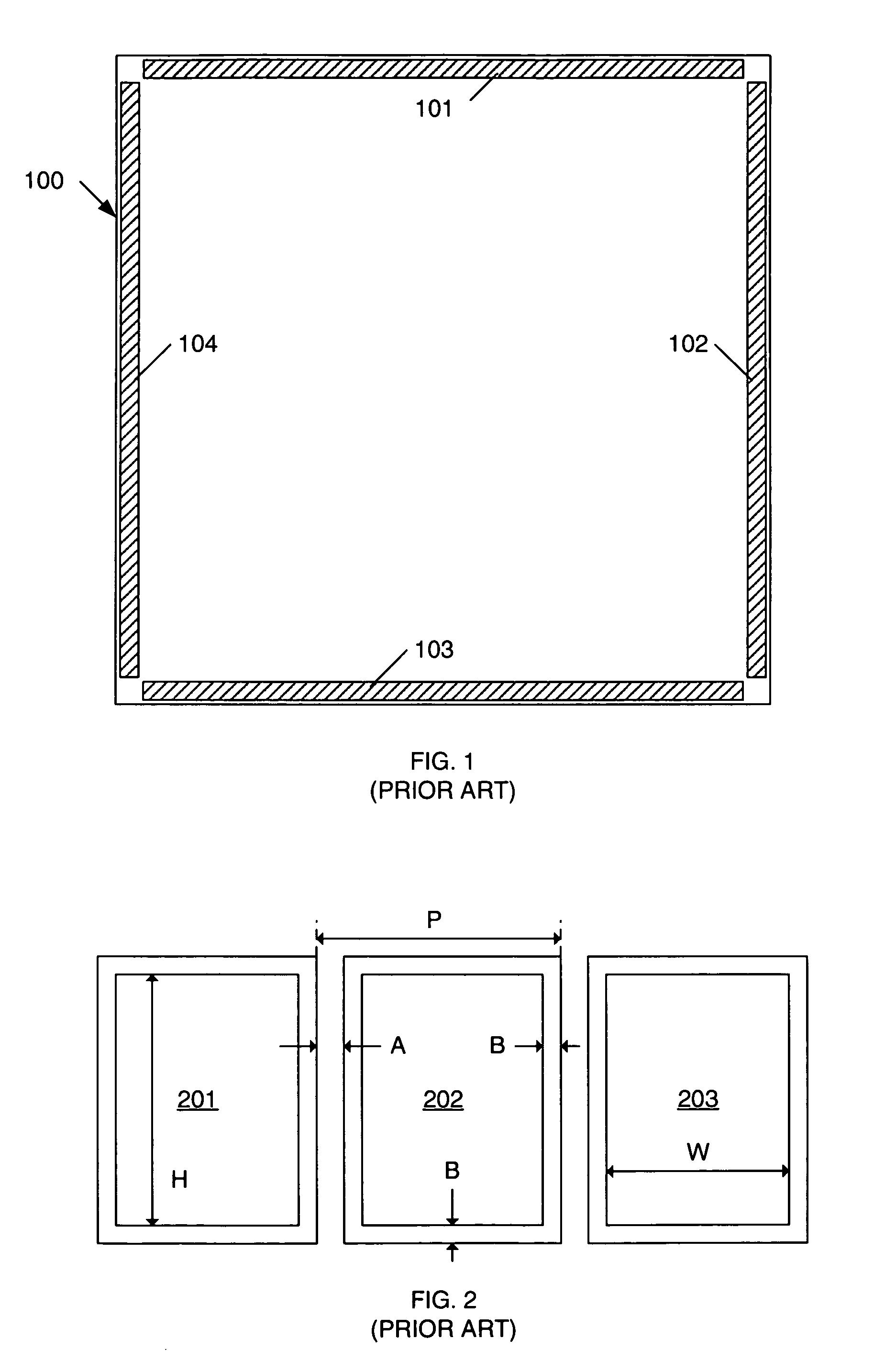
[0030]In general, the present invention provides a bond pad / probe pad layout arrangement that results in a relatively tight pitch through the efficient use of space. More specifically, the present invention includes an elongated pad structure having 2 distinct areas: a bond area and a smaller probe area. These two areas on the same die, are adjacent and are electrically connected to one another. Testing is performed by probing the smaller probe area, and bonding is performed at the larger bond area. The elongated pad structure is repeated, with alternating pad structures being reversed, thereby resulting in a minimum metal-to-metal spacing between adjacent pad structures. This configuration results in a relatively tight pitch, when compared to a simple linear arrangement of pads (see, FIG. 2). The alternating pad structure results in bond areas being located adjacent to probe areas, resulting in tighter pitch than was previously possible. The centers of the probe areas form a regula...
PUM
 Abstract
Description
Claims
Application Information