Phase change-type memory element and process for producing the same

a memory element and phase change technology, applied in the direction of transistors, solid-state devices, instruments, etc., can solve the problems of reducing limiting the production technology for a reduction of the inner diameter of the contact hole, and disadvantageous temperature in the production of transistors or diodes constituting a drive circuit, etc., to achieve the effect of improving the integration density and simply producing

Inactive Publication Date: 2005-02-22
DAI NIPPON PRINTING CO LTD
View PDF3 Cites 299 Cited by
  • Summary
  • Abstract
  • Description
  • Claims
  • Application Information

AI Technical Summary

Benefits of technology

The present invention has been made under these circumstances, and an object of the present invention is to provide a phase change-type memory element, which can reduce a necessary reset pulse current value for returning the phas...

Problems solved by technology

This poses a problem that a large current pulse is necessary as a reset pulse for returning the phase state from the ON state to the OFF state.
Therefore, for example, the temperature in the production of transistors or diodes constituting a drive circuit is disadvantageously restricted.
However, the formation of the contact hole having an inner diameter of 0.1 to ...

Method used


Image

  • Phase change-type memory element and process for producing the same
  • Phase change-type memory element and process for producing the same
  • Phase change-type memory element and process for producing the same

Examples


example 1

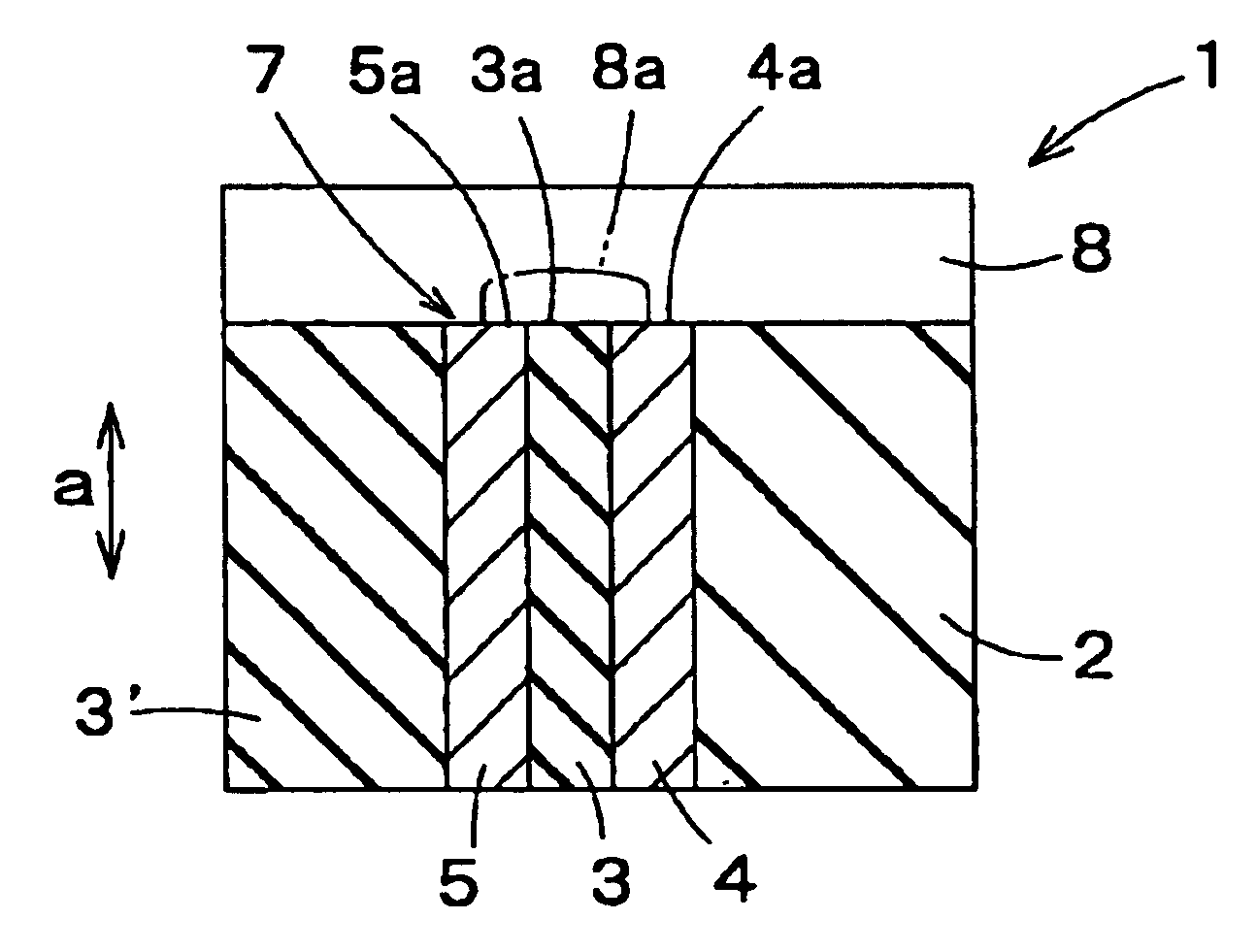
A conductive layer of nickel was formed by sputtering on a glass substrate. The conductive layer was patterned by photography to form a stripe-shaped electrode layer having a thickness of 200 nm and a width of 1.0 μm. Next, an insulating layer of SiO2 was formed by plasma CVD on the glass substrate so as to cover the electrode layer (thickness of the insulating layer on the electrode layer: 200 nm). Thereafter, a conductive layer of nickel was formed by sputtering on the insulating layer 3. The conductive layer was patterned by photography to form a stripe-shaped electrode layer having a thickness of 200 nm and a width of 1.0 μm so that this electrode layer was located opposite to the above electrode layer through the insulating layer. Thus, a laminate structure, in which two 200 nm-thick stripe-shaped electrode layers had been separated by a 200 nm-thick insulating layer, was formed.

An insulating layer of SiO2 (thickness: 0.2 μm) was then formed by plasma CVD on the insulating laye...

example 2

A phase change-type memory element was prepared in the same manner as in Example 1, except that the thickness and the width of the two stripe-shaped electrode layers were changed to 50 nm and 0.5 μm, respectively, and the thickness of the thin layer of the chalcogenide (TeSb) alloy as the phase change recording material layer was changed to 10 nm.

For the phase change-type memory element thus obtained, writing, reading, erasing, and reading were carried out in that order in the same manner as in Example 1. As a result, the average electric resistance value during reading in ON state was about 200 Ω, and the average electric resistance value during reading in OFF state was about 800 Ω. This demonstrates that the phase change-type memory element according to the present invention can reliably function even at a low reset pulse current.

As is apparent from the foregoing detailed description, according to the present invention, a phase change recording material layer is provided on an exp...


PUM


Abstract

There are provided a phase change-type memory element, which can reduce a reset pulse current value necessary for returning the phase state from an ON state to an OFF state, can improve integration density, is not restricted by the process temperature at the time of the production thereof, and can be simply produced, and a process for producing the same. The phase change-type memory element comprises: two or more electrodes provided opposite to each other through an insulating layer; an exposed surface on which at least a part of the insulating layer and at least a part of each of the electrodes are exposed; and a phase change recording material layer provided, on the exposed surface, in contact with the at least two electrodes. The production process of the phase change-type memory element comprises the steps of: providing two or more electrodes opposite to each other through an insulating material; forming an exposed surface on which at least a part of the insulating material and at least a part of each of the electrodes are exposed; and forming a phase change recording material layer on the exposed surface so as to be in contact with at least two of the electrodes.

Description

TECHNICAL FIELDThe present invention relates to an erasable nonvolatile memory element / device, particularly a phase change-type memory element, and a process for producing the same.BACKGROUND OF THE INVENTIONA phase change-type memory element is disclosed in Japanese Patent Laid-Open No. 21740 / 1993. This phase change-type memory element utilizes, as a recording material, an electrically rewritable and erasable phase-change material, for example, a material which enables electrical switching between a substantially amorphous state and a substantially crystalline state or between different resistance states while maintaining the crystalline state.The structure of the phase change-type memory element disclosed in Japanese Patent Laid-Open No. 21740 / 1993 is such that a recording material (a phase change material) is provided between electrodes, and an insulating layer with an opening having a predetermined size is interposed between the electrodes and the recording material. Upon the ap...

Claims


Application Information

Patent Timeline
IPC IPC(8): G11C11/00G11C17/00H01L45/00H01L27/10G11C16/02H01L27/105H01L27/24H01L27/28H01L51/05
CPCG11C13/0004H01L45/06H01L45/1226H01L45/14H01L45/124H01L45/16H01L45/122H01L45/141G11C2213/71H01L27/2409H01L27/2481H10B63/20H10B63/84H10N70/231H10N70/821H10N70/8265H10N70/823H10N70/882H10N70/881H10N70/011
Inventor IDEHARA, TOMOYUKI
Owner DAI NIPPON PRINTING CO LTD
Why Eureka
Try Eureka