

Method to embed thick film components
- Summary
- Abstract
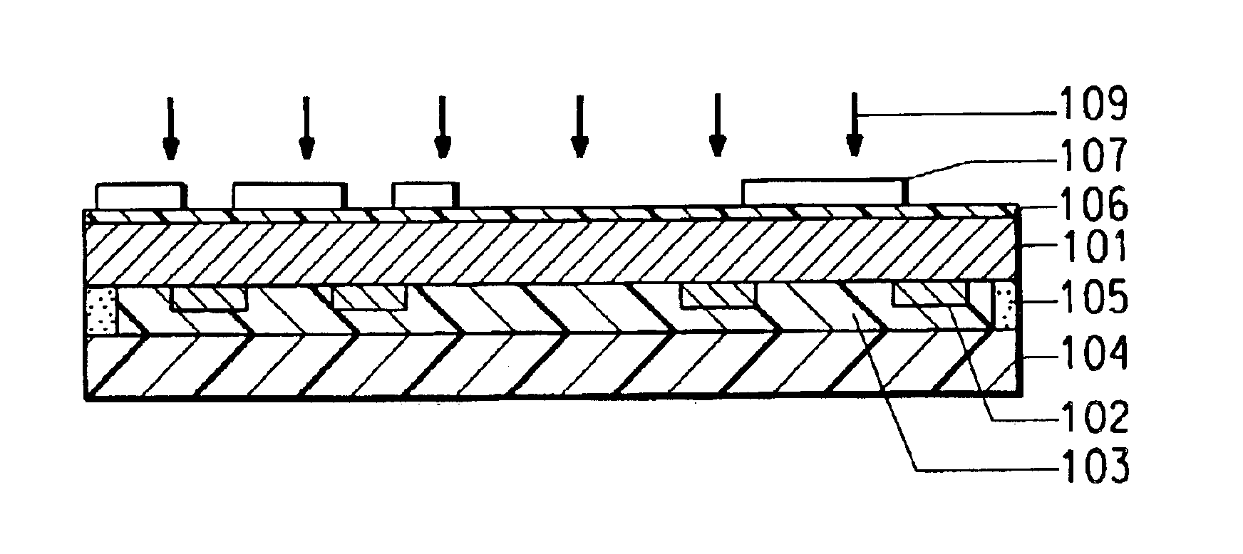
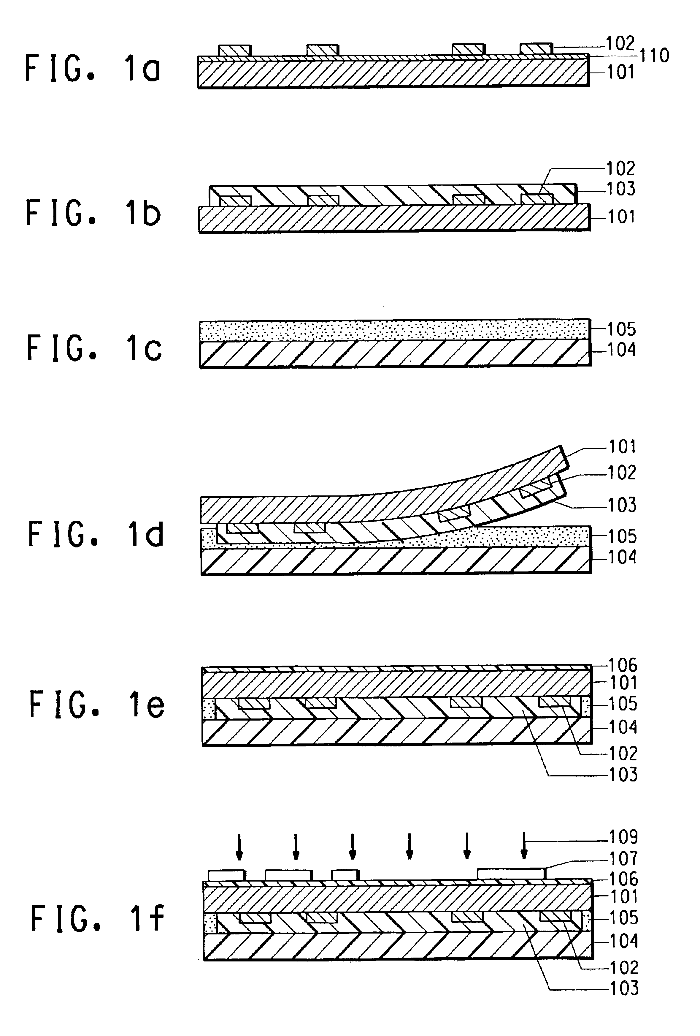
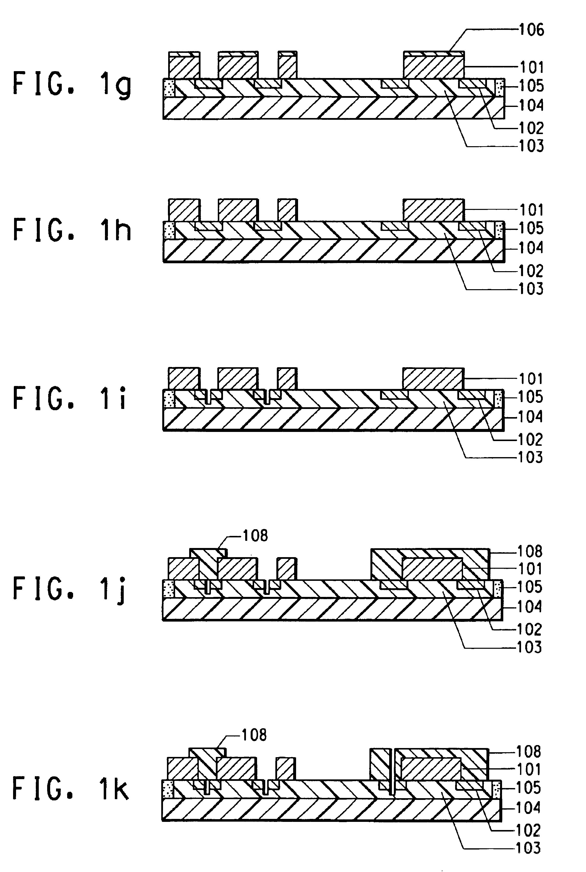
- Description
- Claims
- Application Information
AI Technical Summary
Benefits of technology
Problems solved by technology
Method used
Image

Examples
example 1
The metallic substrate was 1 oz. copper foil. The conductor composition was a copper composition with the following composition:
TEXANOL ®15.00%(by weight)Ethyl Cellulose0.75%Glass A0.60%Spherical Copper83.50%Phosphate Wetting Agent*0.15%*TriDecyl Phosphate
Composition of Glass A:
Silica9.4%(by weight)B2O312.2%Lead Oxide65.9%Cadmium Oxide6.7%Sodium Fluoride3.2%Aluminum Oxide0.2%
The conductor composition was applied by screen-printing and covered nearly the entire foil. It was dried at 130° C. and fired in a belt furnace at a maximum temperature of 900° C. in a nitrogen atmosphere for ten minutes. The total residence time in the furnace was one hour. The resistor composition was DuPont QP602 which is a LaB6 based thick film resistor composition. The thick film resistor composition was screen printed in two sizes of small rectangles on the same metallic substrate: 20×50 mil and 30×55 mil. There were 96 of each size of thick film resistor on the substrate. The resistor composition was dr...
example 2
The process from Example 1 was repeated with the following changes: QP601 (made by The DuPont Company and is a nitrogen fireable 10 ohm / sq LaB6 based resistor composition) was used as the thick film resistor composition; the power settings were 1.2, 1.5, and 1.8 watts; and the target resistance was 14 ohms. The laser trimming did not damage the boards and the cuts in the thick film resistors were clean and accurate. The average percent change in resistance in the post-trim stability test was 1.2%.
PUM
| Property | Measurement | Unit |
|---|---|---|
| Fraction | aaaaa | aaaaa |
| Fraction | aaaaa | aaaaa |
| Fraction | aaaaa | aaaaa |
Abstract
Description
Claims
Application Information