
Multiple chip stack structure and cooling system

Inactive Publication Date: 2005-03-01
MICRON TECH INC
View PDF53 Cites 29 Cited by
  • Summary
  • Abstract
  • Description
  • Claims
  • Application Information

AI Technical Summary

Benefits of technology

Advantageously, the preferred embodiments of the present invention provide an electronic module that is comprised of multiple chip stacks combined into a single, compact module that can be easily installed and removed. Furthermore, the preferred embodiments also provide a cooling system that effectively facilitates heat dissipation from the densely packed module. These and other advantages of the present invention will become more fully apparent from the following description taken in conjunction with the accompanying drawings.

Problems solved by technology

As a result of the increased device density of VLSI (Very-Large-Scale Integration) and ULSI (Ultra-Large-Scale Integration) integrated circuitry, wiring interconnective metallurgy between input / output terminals of stacked integrated circuit chips has become increasingly more complex.
Unfortunately, such dimensional reductions tend to increase the capacitance between adjacent conductors, thereby possibly increasing signal propagation delays and signal cross-talk.
The limitations brought about by capacitive coupling between adjacent conductors has become a significant impediment to achieving higher wiring density.
Consequently, reducing the distance between adjacent leads may adversely impact the functionality of the multi-chip structure due to an increase in the capacitive load between adjacent conductors.
However, the polyimides provide limited improvement for the capacitive coupling problem and, therefore, do not provide a significant advantage in use.
Although air bridge structures permit an increase in the integrated circuit wiring density, the use of air bridges introduces some new problems such as the effective removal of heat from the air bridge structures.
As the cross-sectional area of an air bridge conductor decreases, the electrical resistance of the conductor increases, which results in an increase of the operating temperature of the conductors.
As the number of components in a multi-chip electronic package increases and the packaging density becomes more compact, the ability of heat to dissipate efficiently diminishes, which increases the risk of self-overheating and may reduce the reliable life of the semiconductor device.
Therefore, as the ambient temperature of the package increases due to excessive heat generated by the conductors, hot spots within the multi-chip electronic package may form and adversely affect the performance of the integrated circuit.

Method used


Image

  • Multiple chip stack structure and cooling system
  • Multiple chip stack structure and cooling system
  • Multiple chip stack structure and cooling system

Examples


Embodiment Construction

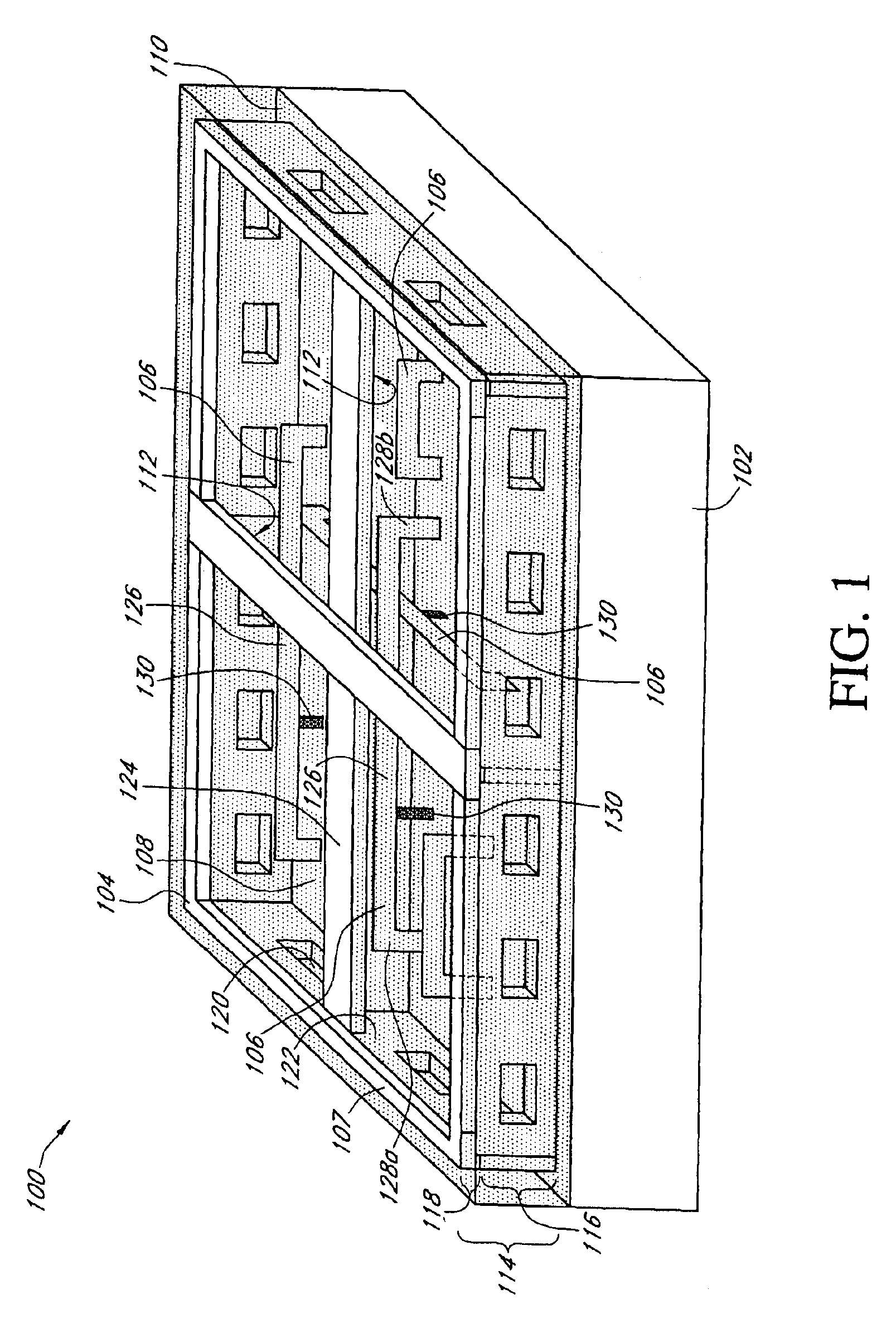
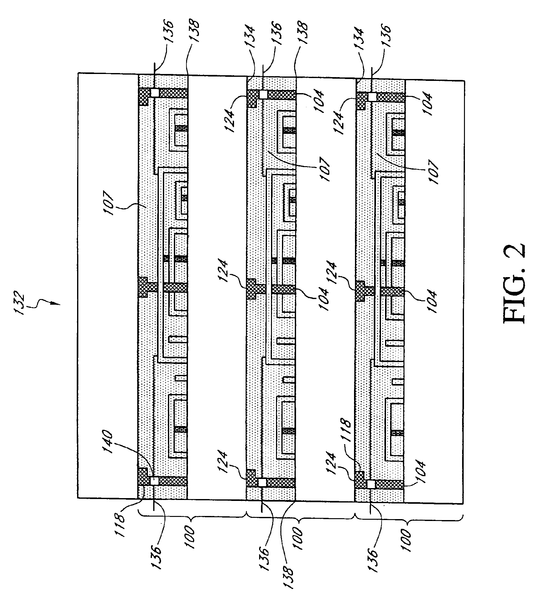
References will now be made to the drawings wherein like numerals refer to like parts throughout. FIG. 1 is a partial schematic illustration of one embodiment of an integrated circuit chip 100 that can be incorporated into a multiple chip stack structure of the preferred embodiment. As shown in FIG. 1, the chip 100 comprises a substrate 102 such as a silicon substrate, that carries a variety of integrated circuitry and devices, such as capacitors, resistors, transistors, memory cells, and logic gates, that are formed using conventional semiconductor manufacturing processes. As also shown in FIG. 1, the chip 100 further comprises a support frame 104, a plurality of air bridge structures 106 and a temporary support material 107 that are each formed on an upper surface 108 of the substrate 102 using methods known in the art or, more preferably, in accordance with methods described in Applicant's co-pending U.S. patent application Ser. No. 09 / 382,929, entitled “PACKAGING OF ELECTRONIC C...


PUM


Abstract

An electronic package comprised of multiple chip stacks attached together to form a single, compact electronic module. The module is hermetically sealed in an enclosure. The enclosure comprises a pressurized, thermally conductive fluid, which is utilized for cooling the enclosed chip stack. A structure that allows for densely-packed, multiple chip stack electronic packages to be manufactured with improved heat dissipation efficiency, thus improving the performance and reliability of the multi-chip electronic packages.

Description

BACKGROUND OF THE INVENTION1. Field of the InventionThe present invention relates to semiconductor processing technology and, in particular, concerns an electronic module comprised of multiple chip stacks assembled into a single electronic package having improved heat dissipation.2. Description of the Related ArtSemiconductor manufacturers continually strive to increase the packaging density of integrated circuit chips, which has led to the development of high-density electronic packaging modules such as three-dimensional multi-chip structures. Multi-chip structures typically comprise a plurality of integrated circuit chips that are adhered together in a stack so as to reduce the amount of space that the chips occupy inside a system. Typically, each chip in the stack has a plurality of conductive input / output contacts that are exposed on at least one lateral surface of the chip. The exposed contacts provide conductive interconnection between the chips in the stack and external circu...

Claims


Application Information

Patent Timeline
IPC IPC(8): H01L25/065
CPCH01L25/0652H01L2225/06589H01L2924/0002H01L2924/00
Inventor FARRAR, PAUL A.ELDRIDGE, JEROME M.
Owner MICRON TECH INC
Features
  • Generate Ideas
  • Intellectual Property
  • Life Sciences
  • Materials
  • Tech Scout
  • Unparalleled Data Quality
  • Higher Quality Content
  • 60% Fewer Hallucinations
Learn More