One transistor DRAM cell structure and method for forming

a technology of dram cells and transistors, applied in the direction of electrical equipment, semiconductor devices, instruments, etc., can solve the problems of achieving both writing and erasing with sufficient speed, and affecting the effect of dram cell structur

Inactive Publication Date: 2005-03-01
III HLDG 12 LLC
View PDF10 Cites 245 Cited by
  • Summary
  • Abstract
  • Description
  • Claims
  • Application Information

AI Technical Summary

Problems solved by technology

One of the difficulties has been in achieving both writing and erasing with sufficient speed.
If the hole removal is not sufficiently faster than hole/electron pair generation in the erase mode, then erase is to...

Method used


Image

  • One transistor DRAM cell structure and method for forming
  • One transistor DRAM cell structure and method for forming
  • One transistor DRAM cell structure and method for forming

Examples


Embodiment Construction

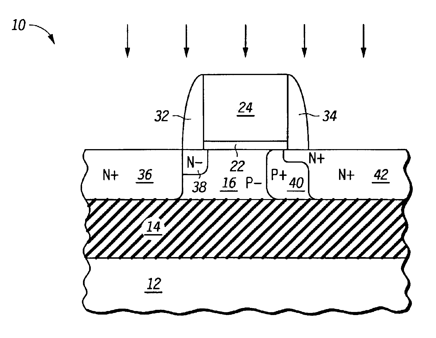
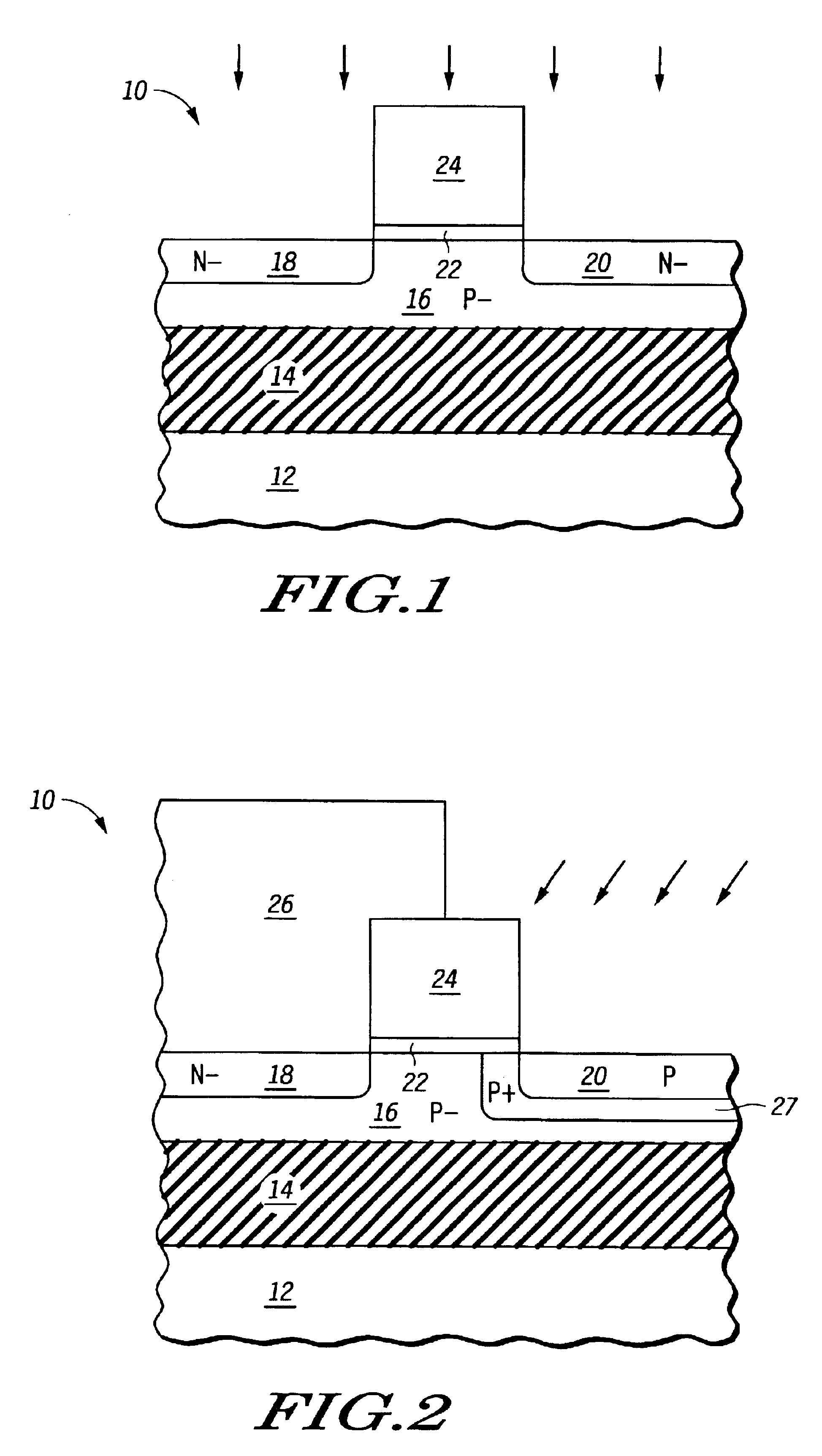
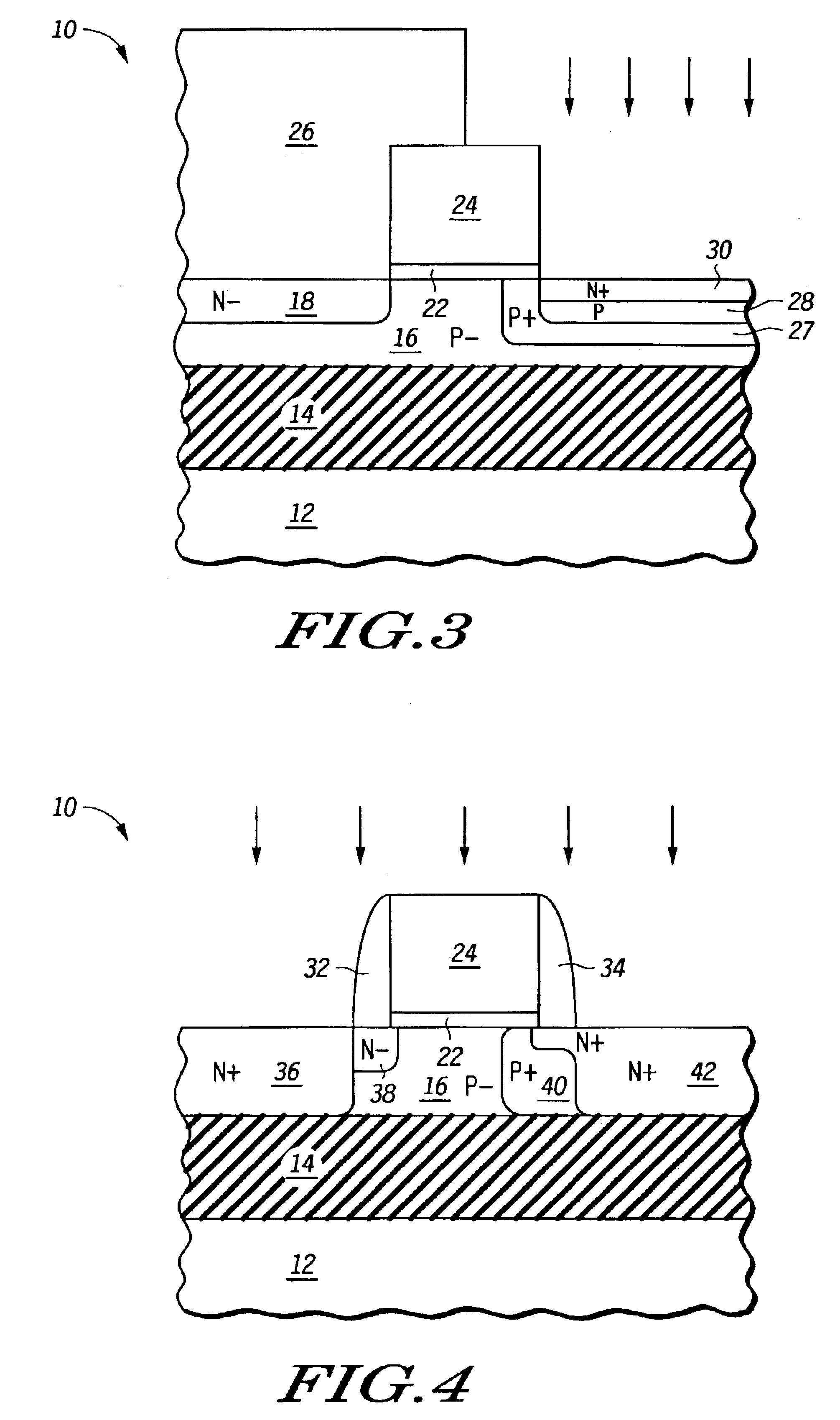
In one embodiment, a single transistor DRAM cell is a transistor formed in a SOI substrate so that the DRAM cells are formed in bodies electrically isolated from each other. Each cell has doped regions that act as source and drain contacts. Adjacent to one of the source and drain contacts and to the body is a region of the same conductivity type as the body but of a higher concentration. Also adjacent to one of the source and drain contacts and to the body is a region of the same conductivity type as the source and drain contacts but of a lower concentration. This is better understood with reference to the drawings and the following description.

Shown in FIG. 1 is a device structure 10 formed in a SOI substrate comprising a substrate 12, an insulator 14 on substrate 12, a body region 16 over insulator 14, a doped region 18, a doped region 20, a gate dielectric 22, and a gate 24. Doped regions 18 and 20 are doped to N− by an implant using gate 24 as a mask. This implant is chosen to b...


PUM


Abstract

A single transistor DRAM cell is formed in a SOI substrate so that the DRAM cells are formed in bodies that are electrically isolated from each other. Each cell has doped regions that act as source and drain contacts. Between the drain contact and the body is a region, which aids in impact ionization and thus electron/hole formation during programming that is the same conductivity type as the body but of a higher concentration than the body. Adjacent to the source contact and to the body is a region, which aids in diode current during erase, that is the same conductivity type as the source contact but of a lower concentration than the source contact.

Description

FIELD OF THE INVENTIONThe present invention relates to dynamic random access memory (DRAM) cells, and more particularly to DRAM cells not requiring a separate capacitor.RELATED ARTDRAMs in general have enjoyed great success primarily due to the high density with good speed. In the quest for even higher density, a technique for single transistor DRAMs has been developed. The individual cell is provided in a semiconductor on insulator (SOI) substrate and requires only a single transistor, doing away with the need for the capacitor that has historically been used in DRAMs. These types of DRAM cells are also known as capacitorless DRAM cells because of not requiring a capacitor. In such a single transistor DRAM cell, the body of the transistor is left floating and, because it is on an SOI substrate so that the bodies of the transistors are isolated from each other, charge is accumulated in the body. This alters the threshold of the transistor, and such difference can be detected.The tec...

Claims


Application Information

Patent Timeline
IPC IPC(8): H01L21/265H01L21/02H01L29/786H01L29/10H01L29/66H01L21/336H01L29/02H01L21/8242H01L21/84H01L27/108H01L27/12
CPCH01L21/26586H01L21/84H01L27/108H01L29/78624H01L27/1203H01L29/1045H01L29/1083H01L29/66659H01L27/10844G11C2211/4016A61P31/04H10B12/01H10B12/00
Inventor BURNETT, JAMES D.
Owner III HLDG 12 LLC
Why Eureka
Try Eureka