Semiconductor cooling device and method of controlling same

Inactive Publication Date: 2005-03-08
PANASONIC CORP
View PDF8 Cites 0 Cited by
  • Summary
  • Abstract
  • Description
  • Claims
  • Application Information

AI Technical Summary

Benefits of technology

By this construction, if the number of revolutions of the inverter-controlled refrigerant pump is increased, a high cooling power can be obtained, making it possible to reduce the size of the refrigerant pump. Also, it is possible to reduce the length of time required to develop different cooling devices by employing the identical inverter-controlled refrigerant pump therein.
In a preferred embodiment of the present invention, the refrigerant is filled in the refrigerating cycle in a quantity equal to 65 to 75% of the volume of the refrigerating cycle. This makes it possible for the interior of the condenser to be in a two phase condition involving a high thermal conductivity and for the refrigerating cycle to maximize the performance of the condenser, making it possible to provide a compact cooling device. It is also possible to secure the refrigerating cycle in which no gas-entrapped operation in which the inverter-controlled refrigerant pump entraps a gas as a result of emergence of a vapor refrigerant from an outlet of the condenser takes place.
The present invention also provides a method of controlling a semiconductor cooling device of the structure discussed above. Specifically, in the practice of this method, in the event that a temperature sensor fitted to the cold plate detects that the temperature of the c

Problems solved by technology

It is well known that some of the semiconductor elements used in, for example, a computer generate a substantial quantity of heat as the computing speed thereof increases.
However, the capability of the cooling device to cool the semiconductor elements has now come to a limitation.
This heat-pipe type cooling device would involve an increase in size or insufficient cooling performance particularly when it is used in cooling highly exothermic semiconductor elements.
The conventional air-cooling device utilizing the fan and the heat sink is effective to cool a semiconductor of about 70 W. However, when it comes to cooling of a semiconductor element of 150 W or higher, the cooling device tends to become too bulky for it to be incorporated within a rack-type frame structure.
On the other hand, the system in which the semiconductor elements are immersed in the refrigerant such as disclosed in Japanese Laid-open Patent Publication No. 5-315488 di

Method used


Image

  • Semiconductor cooling device and method of controlling same
  • Semiconductor cooling device and method of controlling same
  • Semiconductor cooling device and method of controlling same

Examples


Embodiment Construction

This application is based on an application No. 2002-121919 filed Apr. 24, 2002 in Japan, the content of which is herein expressly incorporated by reference in its entirety.

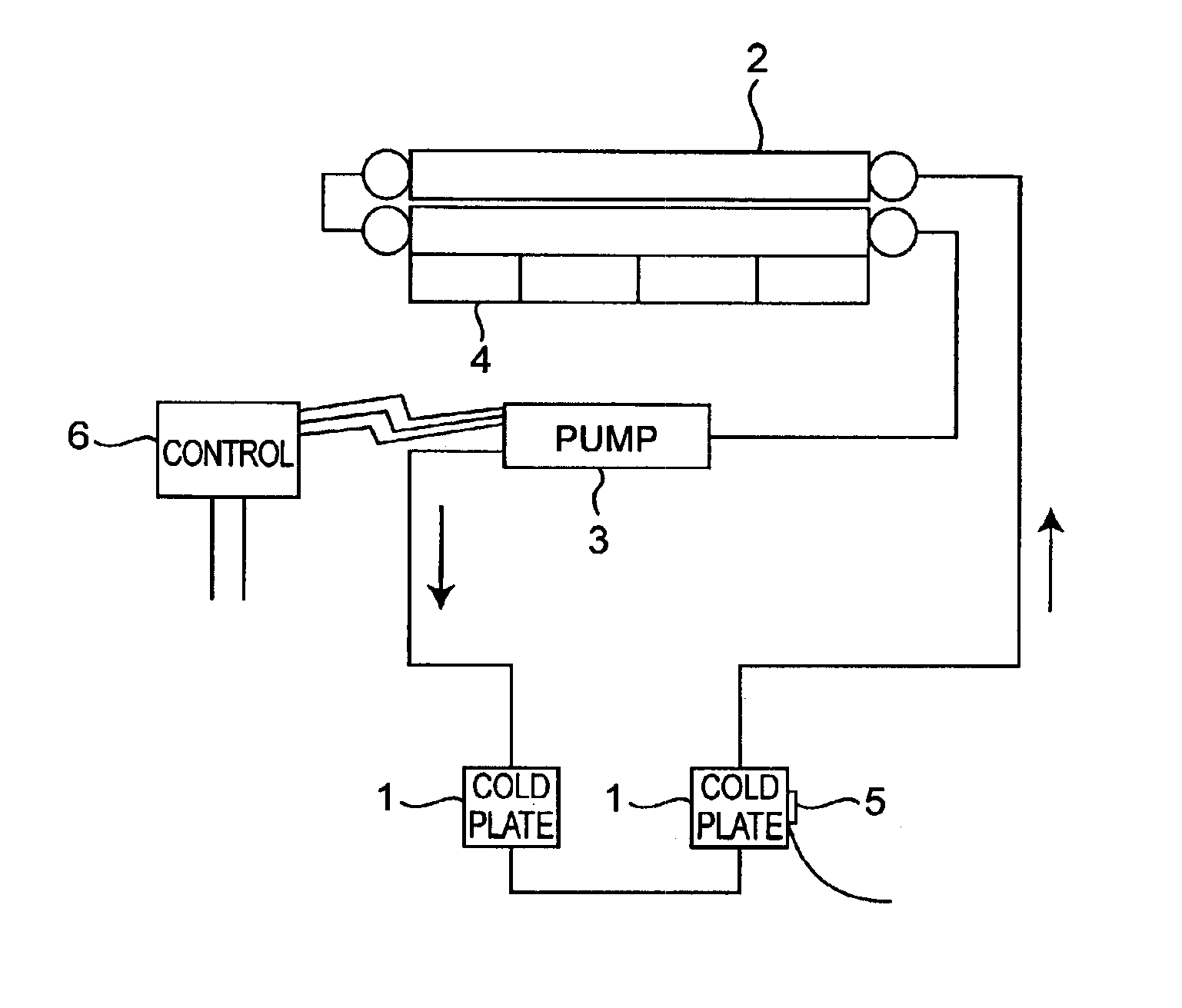
Referring first to FIG. 1 showing a refrigerating cycle employed in the present invention, a cooling device includes a plurality of (for example, two) cold plates 1 for cooling highly exothermic semiconductor elements, that is, semiconductor elements tending to emit a substantial amount of heat when in operation, a condenser 2, and an inverter-controlled refrigerant pump 3, all connected in series with each other to define a refrigerating cycle. A refrigerant is filled in this refrigerating cycle. The condenser 2 is adapted to be cooled by a fan 4.

The cooling device is so designed that the refrigerant emerging first from the condenser 2 is supplied towards the cold plates 1 by the refrigerant pump 3. The cold plates 1 so supplied with the refrigerant absorb heat generated by the highly exothermic semiconductor el...


PUM


Abstract

A semiconductor cooling device includes at least one cold plate for cooling a semiconductor element, a condenser adapted to be cooled by a fan, and a refrigerant pump. The refrigerant pump is electrically connected to an inverter controller that controls the number of revolutions of the refrigerant pump.

Description

BACKGROUND OF THE INVENTION1. Field of the InventionThe present invention relates generally to a cooling device for cooling semiconductor elements which generate a substantial quantity of heat and, in particular but not exclusively, to a compact, easy-to-handle and efficient cooling device for cooling such semiconductor elements by utilization of a change in phase between a liquid phase and a vapor phase of a refrigerant.2. Description of the Related ArtIt is well known that some of the semiconductor elements used in, for example, a computer generate a substantial quantity of heat as the computing speed thereof increases. A cooling device including a fan and a heat sink is generally utilized to cool the semiconductor elements. However, the capability of the cooling device to cool the semiconductor elements has now come to a limitation.In the case of a large-scale computer, Japanese Laid-open Patent Publication No. 5-315488 suggests a method for emergent supply of a refrigerant, but ...

Claims


Application Information

Patent Timeline
IPC IPC(8): F25B49/02H01L23/473H01L23/34H05K7/20F25B5/04F25B5/00F25D11/00F25B1/00H01L23/427
CPCF25B49/025H01L23/473F25B5/04F25B2500/24F25B2600/021F25B2700/2117H01L2924/0002Y02B30/741H01L2924/00Y02B30/70
Inventor NAKANO, MASAOASHITANI, HIROMASA
Owner PANASONIC CORP
Why Eureka
Try Eureka