Chromeless phase shift mask using non-linear optical materials

a phase shift mask and non-linear optical material technology, applied in the field of attenuating phase shift mask formation, can solve the problems of insufficient intensity of light transmitted through the mosi pattern, insufficient opaqueness, sharp edges, etc., and achieve sufficient opaqueness and avoid the effect of using a chrome layer on the mask

Inactive Publication Date: 2005-03-08
BELL SEMICON LLC
View PDF1 Cites 14 Cited by
  • Summary
  • Abstract
  • Description
  • Claims
  • Application Information

AI Technical Summary

Benefits of technology

To achieve the foregoing, the present invention provides methods and photomasks for patterning layers on wafers using a single material for producing both the patterns and fiducials. A non-linear optical material is used in place of existing attenuated phase shift films as a way to avoid using a chrome layer on the mask. Thus, the mask contains only one type of film, namely the non-linear optical material, which accom

Problems solved by technology

The light that is transmitted through the MoSi pattern has an intensity that is insufficient to expose the resist.
That is, the edges become sharper as a result of the small amount of 180-degree phase shifted light destructively interfering with the light passing through the feature.
This is necessitated because the phase shifting films currently used in this scheme (such as MoSi and TiN/SiN) are not sufficiently opaque at the wavelengths that the stepper uses for the above functions.
While these materials provide good phase shifting and contrast at the exposure wavelengths (

Method used


Image

  • Chromeless phase shift mask using non-linear optical materials
  • Chromeless phase shift mask using non-linear optical materials
  • Chromeless phase shift mask using non-linear optical materials

Examples


Embodiment Construction

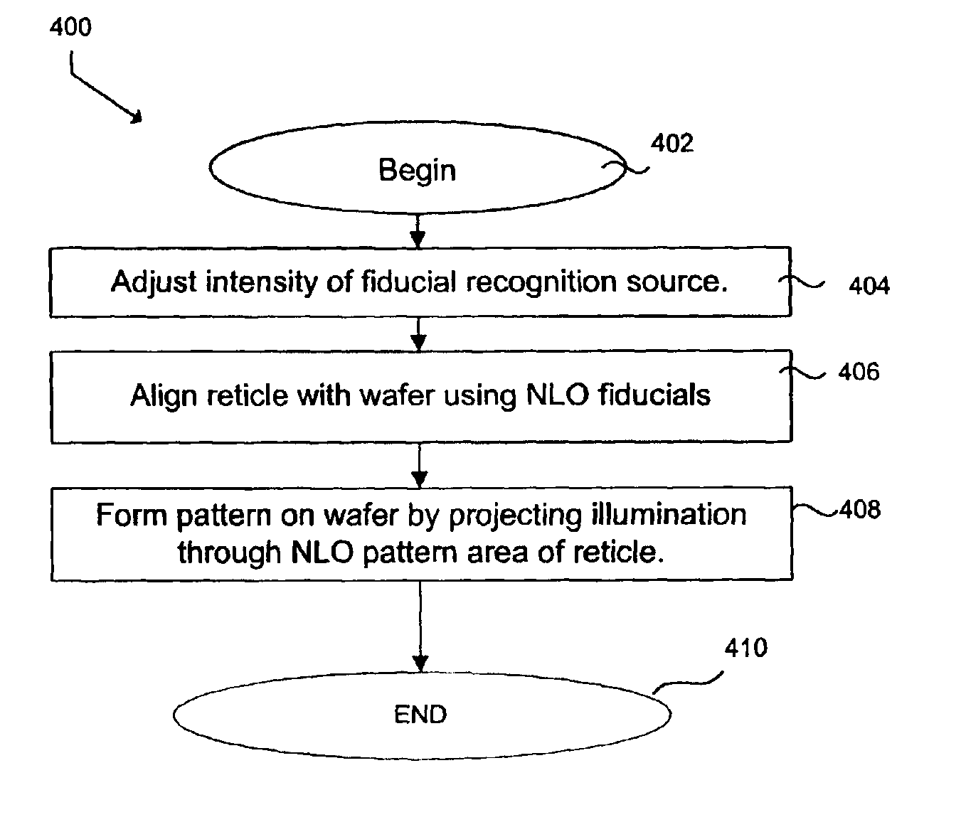
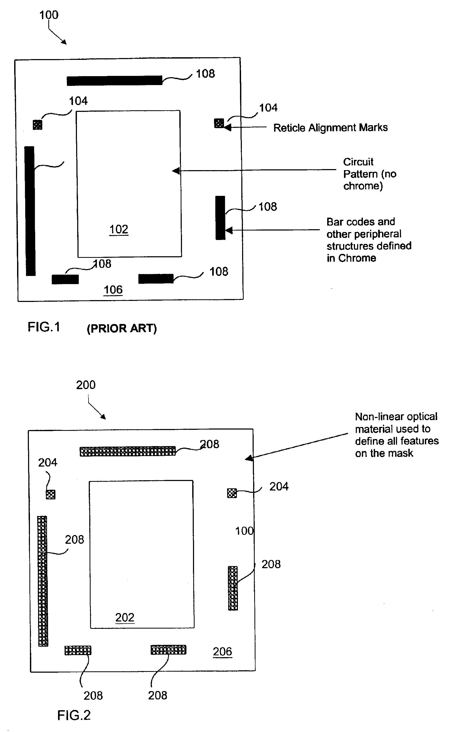
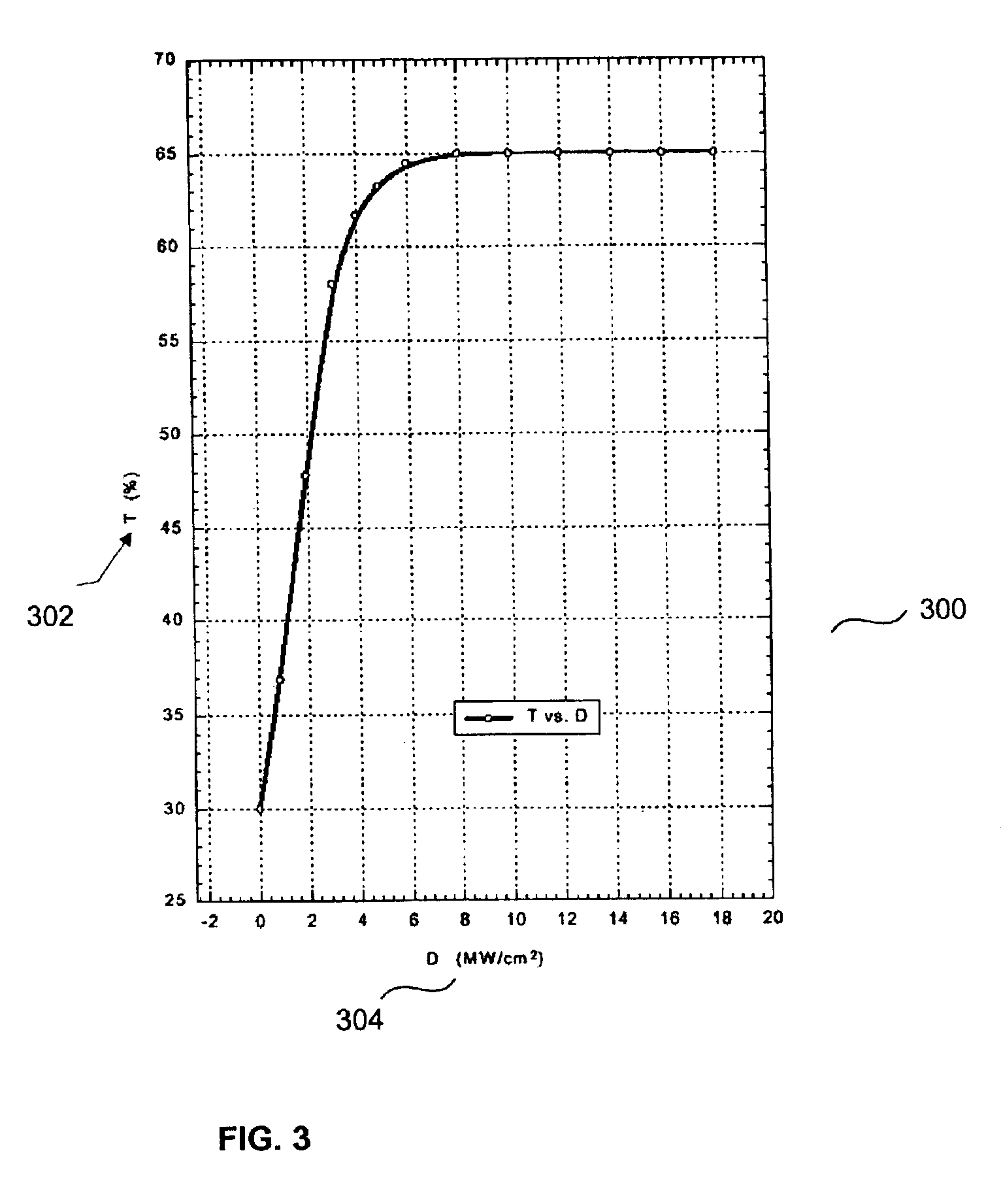
Reference will now be made in detail to preferred embodiments of the invention. Examples of the preferred embodiments are illustrated in the accompanying drawings. While the invention will be described in conjunction with these preferred embodiments, it will be understood that it is not intended to limit the invention to such preferred embodiments. On the contrary, it is intended to cover alternatives, modifications, and equivalents as may be included within the spirit and scope of the invention as defined by the appended claims. In the following description, numerous specific details are set forth in order to provide a thorough understanding of the present invention. The present invention may be practiced without some or all of these specific details. In other instances, well known process operations have not been described in detail in order not to unnecessarily obscure the present invention.

The present invention provides methods and photomasks for patterning layers on wafers usin...


PUM


Abstract

An attenuated phase shift mask is formed using a non-linear optical material for both fiducial features and pattern features. The non-linear optical material selected has predetermined transmission at the actinic exposure wavelength and a smaller transmission at the fiducial recognition wavelengths.

Description

BACKGROUND OF THE INVENTION1. Field of the InventionThe present invention relates to the formation of patterns on photolithography masks used to form patterns on semiconductor wafers. More particularly, the present invention relates to the formation of attenuating phase shift masks used for the fabrication of semiconductor integrated circuits.2. Description of the Related ArtSemiconductor wafer fabrication involves a series of processes used to create semiconductor devices and integrated circuits (ICs) in and on a semiconductor wafer surface. Fabrication typically involves the basic operations of layering and patterning, together with others such as doping, and heat treatments. Layering is an operation used to add thin layers of material (typically insulator, semi-conductor or conductor) to the surface of the semiconductor wafer. Patterning is an operation that is used to remove specific portions of the top layer or layers on the wafer surface. Patterning is usually accomplished thr...

Claims


Application Information

Patent Timeline
IPC IPC(8): G03F9/00G03F1/00G03F1/08G03F1/10G03F1/14
CPCG03F1/14G03F1/56G03F1/44G03F1/32
Inventor TARAVADE, KUNALCALLAN, NEAL
Owner BELL SEMICON LLC
Why Eureka
Try Eureka