Method for forming an optical printed circuit board

a printed circuit board and optical technology, applied in the field of printing circuit board manufacturing, can solve the problems of high manufacturing cost, difficult and manual laborious integration of optical, electronic and optoelectronic components, and bottlenecks in electrical interconnection, so as to improve the clock speed of electrical components, eliminate bottlenecks, and high-speed optical communication

Inactive Publication Date: 2005-03-08
LOCKHEED MARTIN CORP
View PDF13 Cites 16 Cited by
  • Summary
  • Abstract
  • Description
  • Claims
  • Application Information

AI Technical Summary

Benefits of technology

Embodiments of the invention provide a number of technical advantages. Embodiments of the invention may include all, some, or none of these advantages. In one embodiment, a manufacturing method achieves high-speed optical communication between different sections of a printed circuit board. This eliminates any bottlenecks that may occur as a result of increasing clock speeds for electrical components. The manufacturing method results in low-cost optical printed circuit board integration that combines both optical, electrical, and optoelectronic components in a single heterogeneous package. The manufacturing method is also particularly suitable for flex circuits that have thin substrates.

Problems solved by technology

The use of optoelectronic components resulted from the continuing increase in clock speed of the electronic components, which resulted in electrical interconnect bottlenecks, especially in the context of long interconnect bus architecture.
However, the integration of optical, electronic, and optoelectronic components has been difficult and very manual labor intensive, which results in high manufacturing costs and low volume throughput.

Method used


Image

  • Method for forming an optical printed circuit board
  • Method for forming an optical printed circuit board
  • Method for forming an optical printed circuit board

Examples


Embodiment Construction

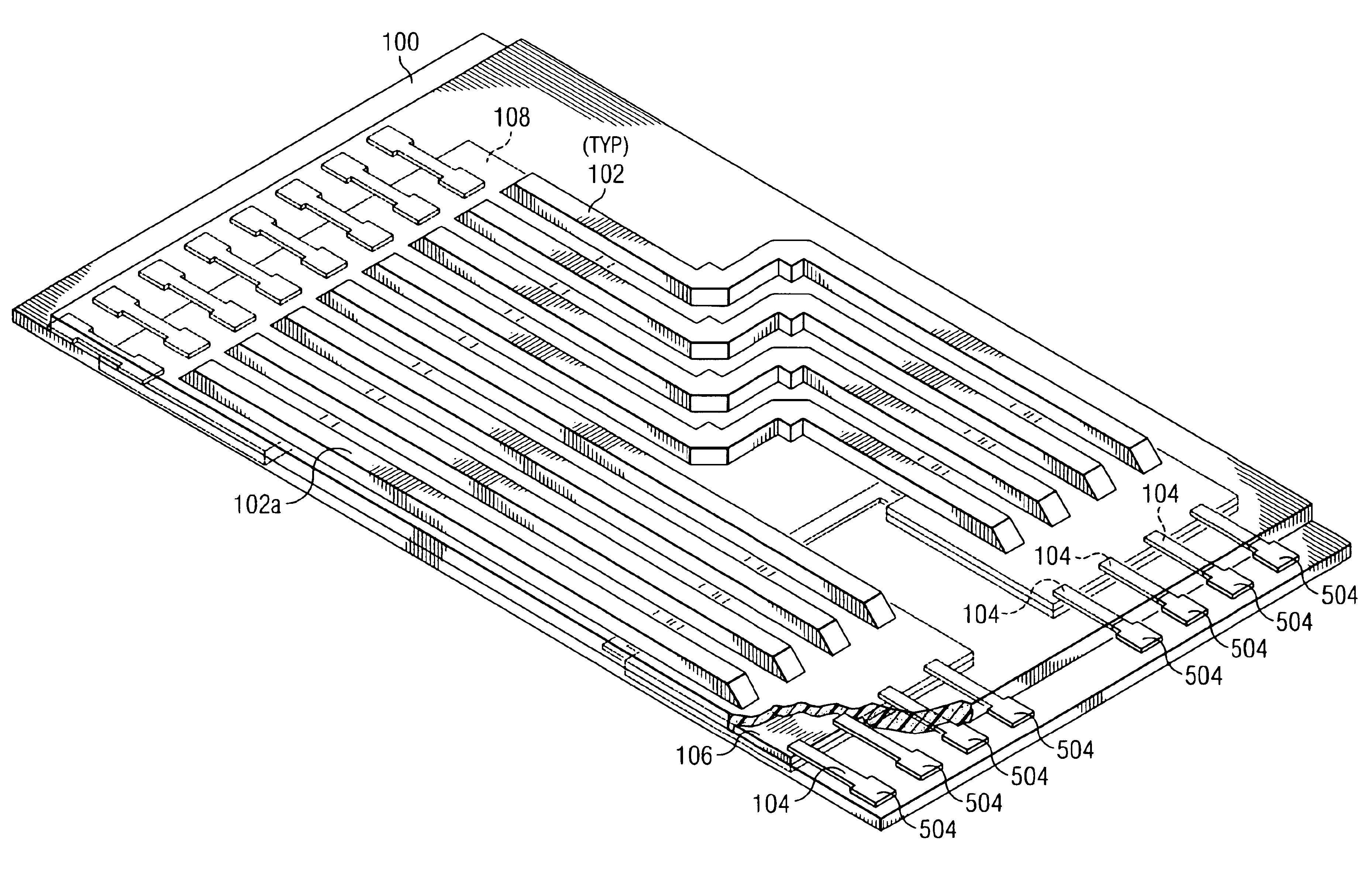
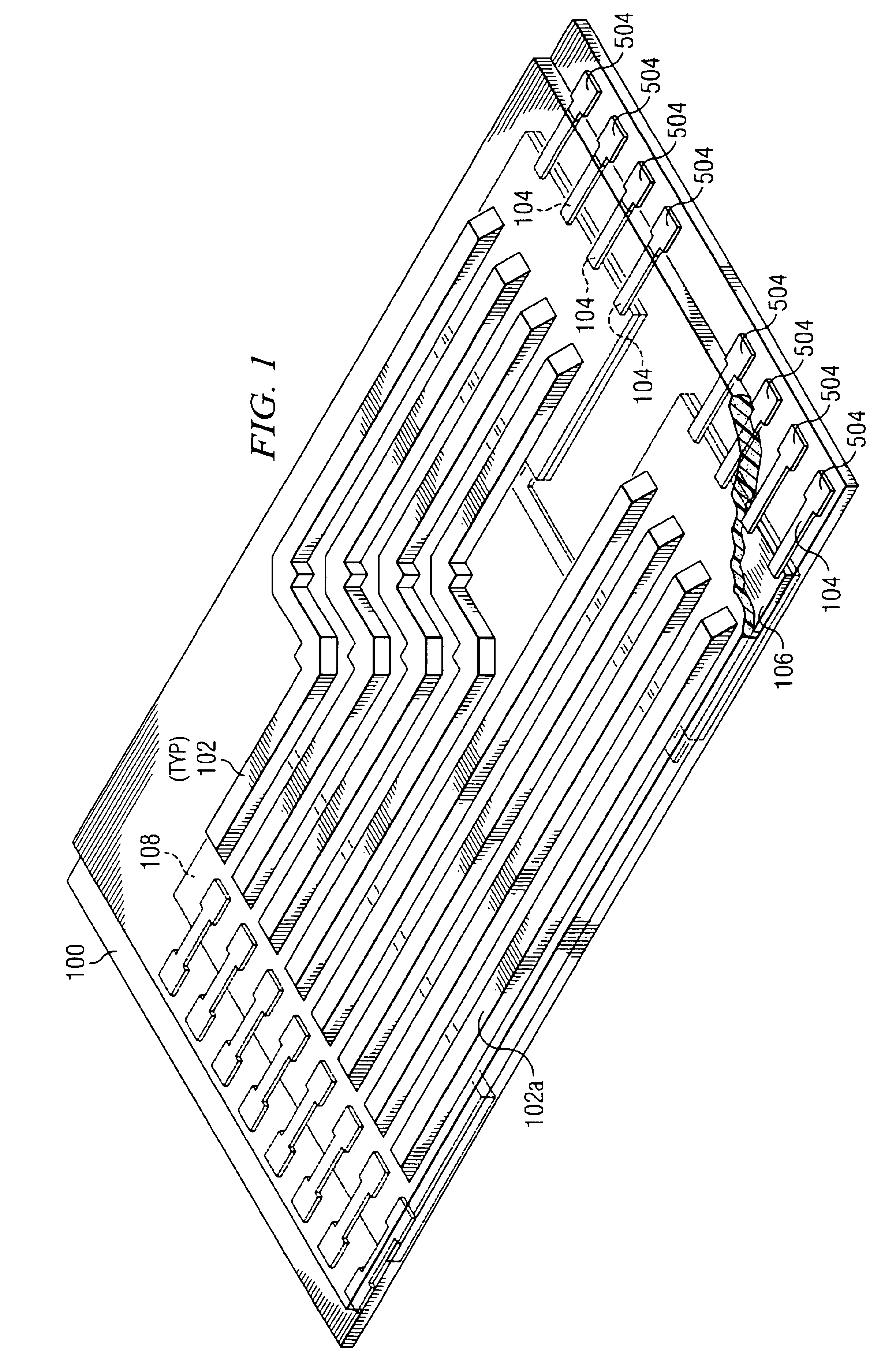
FIG. 1 is a perspective view of a printed circuit board (“PCB”) 100 having one or more optical waveguides 102 formed thereon according to an embodiment of the present invention. PCB 100 is described in greater detail below in conjunction with FIGS. 2 through 7. Generally, PCB 100 includes a plurality of electronic and optoelectronic components coupled thereto that are connected to one another by a plurality of metal traces 104 in such a manner as to form one or more electrical circuits. An example of PCB 100 is a mother board for a computer; however, the present invention contemplates PCB 100 representing any circuit board, printed wiring board, flex circuit, or other suitable substrate having electronic and optoelectronic components coupled thereto. PCB 100 may have any suitable size and any suitable shape and may be formed form any suitable material.

Waveguides 102 are formed by any suitable arrangement of optically transmissive material that communicates optical signals as guided ...


PUM


Abstract

According to one embodiment of the invention, a method includes providing a printed circuit board having a plurality of optoelectronic components coupled to a first side of the printed circuit board, forming a first clad layer outwardly from the first side of the printed circuit board, coupling an injection molding mold to the first side of the printed circuit board, injecting a material into the mold in liquid form, and after the material is solidified, decoupling the injection molding mold from the first side of the printed circuit board, thereby forming an optical waveguide outwardly from the first clad layer. The method may also include forming a second clad layer outwardly from the optical waveguide, and forming a metal layer outwardly from the second clad layer. In lieu of injection molding, stamping may be performed to form the core layer of the optical waveguide.

Description

TECHNICAL FIELD OF THE INVENTIONThe present invention relates generally to the field of printed circuit board manufacturing and, more particularly, to a method for forming an optical printed circuit board.BACKGROUND OF THE INVENTIONPrinted circuit boards are used in many applications, including cell phones, stereo equipment, and computers, just to name a few. Nowadays, the components associated with these printed circuit boards include electronic as well as optoelectronic components. The use of optoelectronic components resulted from the continuing increase in clock speed of the electronic components, which resulted in electrical interconnect bottlenecks, especially in the context of long interconnect bus architecture. However, the integration of optical, electronic, and optoelectronic components has been difficult and very manual labor intensive, which results in high manufacturing costs and low volume throughput.SUMMARY OF THE INVENTIONAccording to one embodiment of the invention,...

Claims


Application Information

Patent Timeline
Patent Type & Authority Patents(United States)
IPC IPC(8): G02B6/122G02B6/43H05K1/02
CPCG02B6/1221H05K1/0274G02B6/43H05K2203/1327
Inventor MA, KELVINTOLLIVER, TODD R.SODERBERG, JOHN J.
Owner LOCKHEED MARTIN CORP
Why Eureka
Try Eureka