

Optical communication device
a communication device and optical technology, applied in the field of optical communication devices, can solve the problems of long, thick, bulky, and large overall size of the ld/pd module of fig. 11, and achieve the effects of shortening the wiring, improving high speed performance, and high speed optical communication
- Summary
- Abstract
- Description
- Claims
- Application Information
AI Technical Summary
Benefits of technology
Problems solved by technology
Method used
Image

Examples
embodiment 1
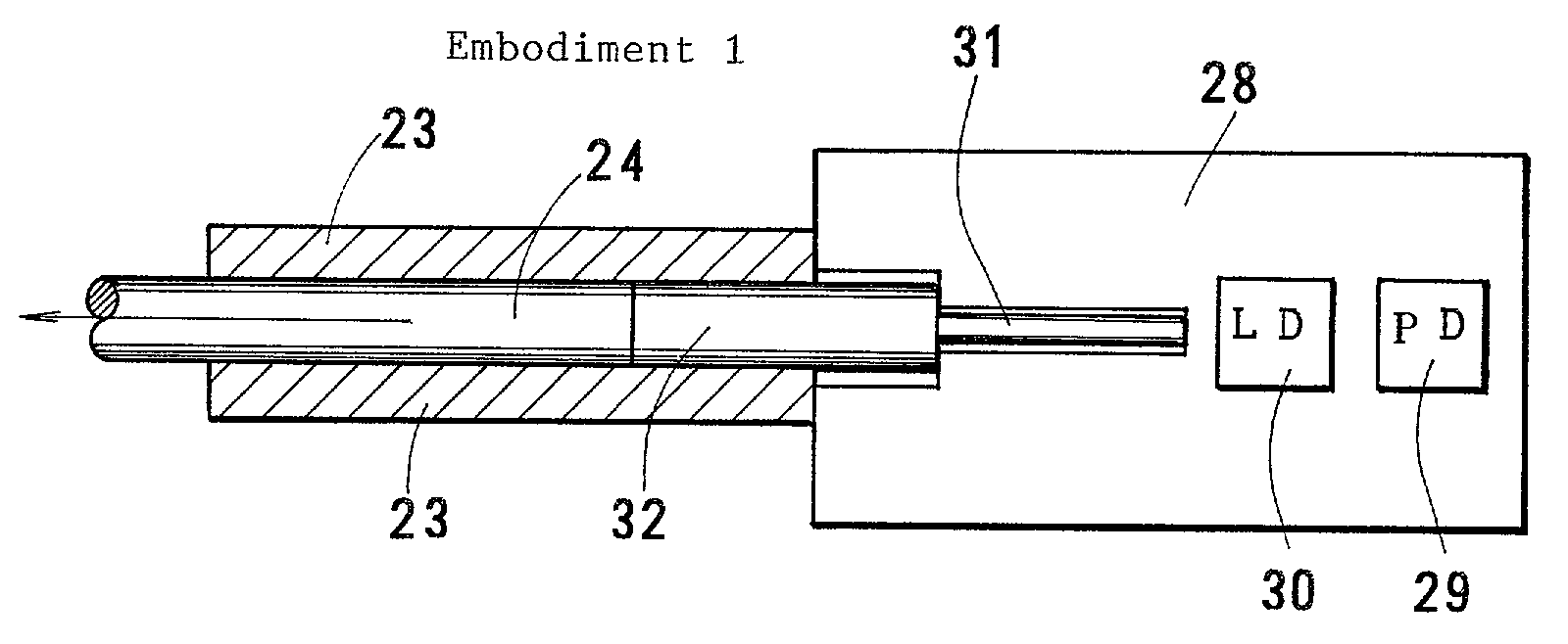
[0062] FIG. 6 and FIG. 7 are an enlarged horizontal view and a vertical section of the optoelectronic (LD) element of As mentioned before, the optoelectronic element 21 includes an LD 30 and a monitoring PD 29. A silicon single crystal bench 28 is employed as a base of the optoelectronic elements. The Si bench 28 as a base only for the optoelectronic elements should not be confused with the circuit board 20 as a base for the whole of the module. The bench 28 is a (100) silicon single crystal. Anisotropic chemical etching forms a bigger V-groove and a smaller V-groove in series along the center line on the silicon bench 28. Marks are made by photolithography at the points at which the LD 30 and the PD 29 should be attached. The marks and the V-grooves ensure exact coupling between the fiber and the LD, which is called "passive alignment". Wiring metallized patterns are made upon the silicon bench 28 by printing, evaporation or sputtering. The LD 30 and the monitoring PD 29 are mount...
embodiment 2
; Receiving Module (PD Module); FIG. 4, FIG. 5, FIG. 8, FIG. 9
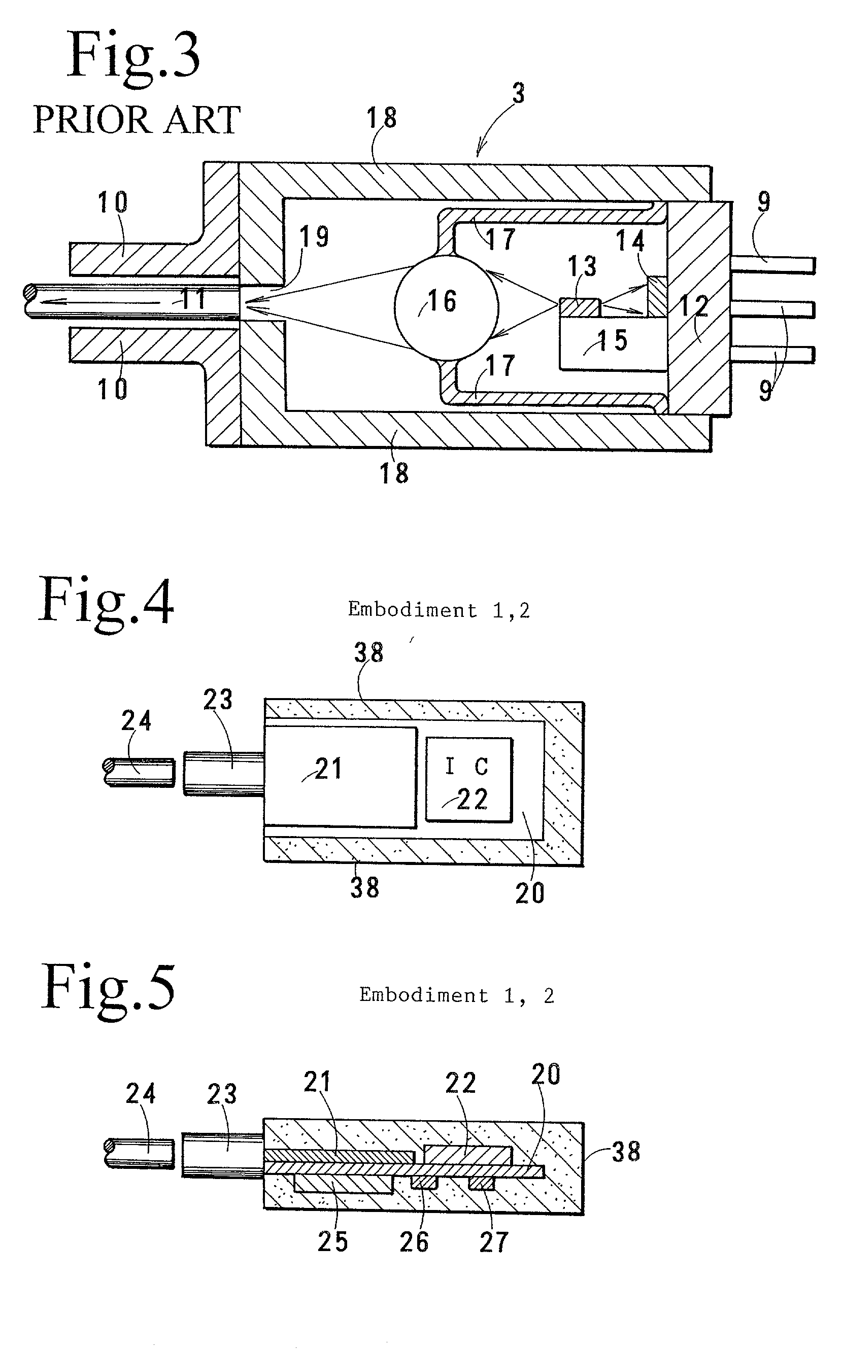
[0064] Embodiment 2 is an example of receiving (PD) modules. FIG. 4 and FIG. 5 show horizontally and vertically sectioned views of Embodiment 2. The figures are common to Embodiments 1 and 2. But substances of the optoelectronic element 21 and the ICs 22 and 25 are different. Like Embodiment 1, Embodiment 2 has a circuit board 20 with a top surface and a bottom surface with metallized patterns. An optoelectronic element 21 and a first IC 22 are loaded serially upon the top surface of the circuit board 20. A second IC 25 and R / C elements 26 and 27 are fitted on a bottom surface of the circuit board 20. A plastic case 38 encloses the circuit board 20, the ICs 22 and 25, the R / C elements 26 and 27 and the optoelectronic element 21. A receptacle 23 with an axial opening is fitted at a front end of the circuit board 20. An end of an optical fiber 24 can be inserted into the receptacle 23.
[0065] The optoelectronic element 21 co...
embodiment 3
; Transmitting / receiving (LD / PD) Module; FIG. 10
[0072] Paired transmitting / receiving (LD / PD) modules are of great use to optical communications. FIG. 10 shows Embodiment 3 as an LD / PD module. Like the Prior Art (LD / PD) of FIG. 11, Embodiment 3 pairs a transmitting (LD) part and a receiving (PD) part in parallel side by side.
[0073] As shown in FIGS. 4 and 5, the transmitting part includes a circuit board 20 with a top metallized patterns and bottom metallized patterns, an LD element 21 and a first IC 22 laid upon the top of the circuit board 20, and a second IC 25 and R / C elements 26 and 27 fitted on the bottom of the circuit board 20. The LD element 21 has an LD and a monitoring PD as depicted in FIG. 6 and FIG. 7. The ICs 22 and 25 indicate an LD driving IC, or an APC (auto power controlling) IC and so on.
[0074] The receiving part includes a circuit board 20' with top metallized patterns and bottom metallized patterns, a PD element 21' and a first IC 22' laid upon the top of the ci...
PUM
 Abstract
Description
Claims
Application Information