
Optical communication device

a communication device and optical technology, applied in the field of optical communication devices, can solve the problems of unfavorable reducing cost and size, long ld/pd modules, and large ld/pd modules, etc., to improve high speed performance, improve high frequency performance, and shorten the wiring

Inactive Publication Date: 2006-11-14
SUMITOMO ELECTRIC IND LTD
View PDF8 Cites 18 Cited by
  • Summary
  • Abstract
  • Description
  • Claims
  • Application Information

AI Technical Summary

Benefits of technology

This approach results in significantly reduced module size, cost, and improved high-speed performance, with the ability to achieve 2.5 Gbps or 5 Gbps transmission, and potentially 10 Gbps under optimal conditions, while enhancing reliability and noise resistance.

Problems solved by technology

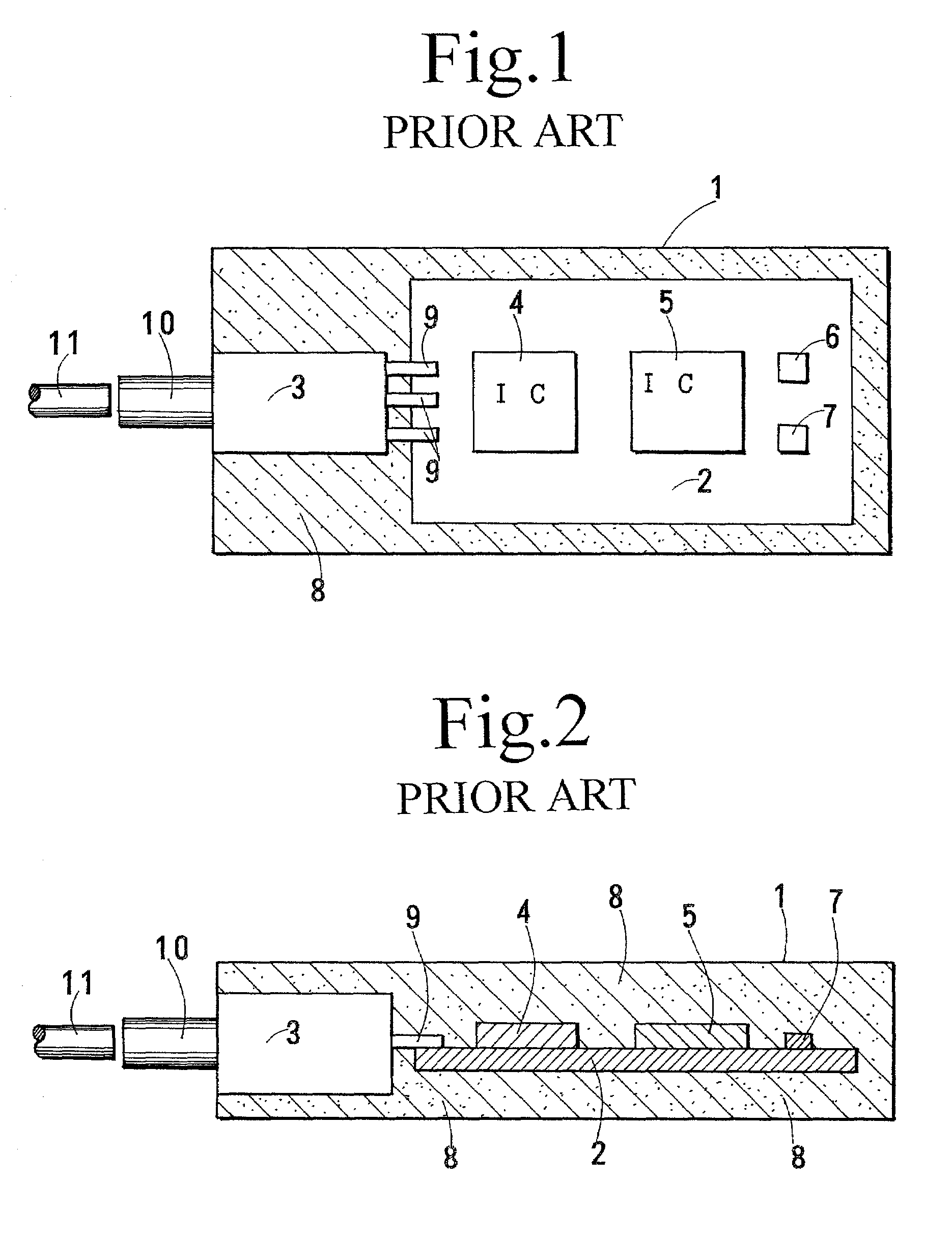
The LD / PD module of FIG. 11 is too long, too wide and too thick.
The module is long, thick and bulky.
Such an LD module or a PD module is unfavorable for reducing cost and size.
Blunt replacement of the metal packaged module by the PLC module is insignificant.

Method used


Image

  • Optical communication device
  • Optical communication device
  • Optical communication device

Examples


embodiment 1

[Embodiment 1; Transmitting Module (LD Module); FIG. 4, FIG. 5, FIG. 6, FIG. 7]

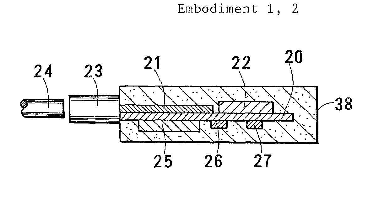
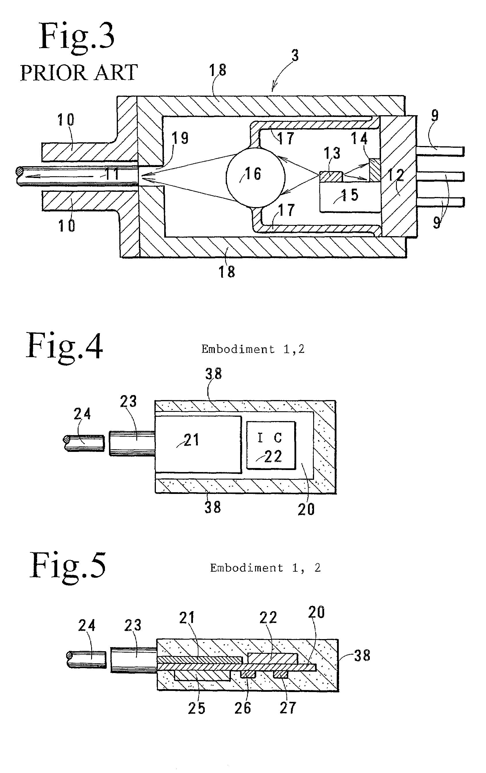
[0059]This invention can be applied to a transmitting (LD) module, a receiving (PD) module and a transmitting / receiving (LD / PD) module. Embodiment 1 is a transmitting (LD) module. FIG. 4 is a horizontally sectioned view of Embodiment 1. FIG. 5 is a vertically sectioned view. Embodiment 1 has a circuit board 20, an optoelectronic element 21, a first IC 22 mounted in series upon a top surface of the circuit board 20, a second IC 25 and R / C elements 26 and 27 mounted on a bottom surface of the circuit board 20, a receptacle 23, and a plastic molding package 38. The plastic package 38 encloses the circuit board 20, the ICs 22 and 25, the R / C elements 26 and 27, and the optoelectronic element 21. The receptacle 23 with an axial opening is fitted at a front end of the circuit board 20. An end of an optical fiber 24 can be inserted into the receptacle 23.

[0060]The optoelectronic element 21 contains a set of a la...

embodiment 2

[Embodiment 2; Receiving Module (PD Module); FIG. 4, FIG. 5, FIG. 8, FIG. 9]

[0064]Embodiment 2 is an example of receiving (PD) modules. FIG. 4 and FIG. 5 show horizontally and vertically sectioned views of Embodiment 2. The figures are common to Embodiments 1 and 2. But substances of the optoelectronic element 21 and the ICs 22 and 25 are different. Like Embodiment 1, Embodiment 2 has a circuit board 20 with a top surface and a bottom surface with metallized patterns. An optoelectronic element 21 and a first IC 22 are loaded serially upon the top surface of the circuit board 20. A second IC 25 and R / C elements 26 and 27 are fitted on a bottom surface of the circuit board 20. A plastic case 38 encloses the circuit board 20, the ICs 22 and 25, the R / C elements 26 and 27 and the optoelectronic element 21. A receptacle 23 with an axial opening is fitted at a front end of the circuit board 20. An end of an optical fiber 24 can be inserted into the receptacle 23.

[0065]The optoelectronic e...

embodiment 3

[Embodiment 3; Transmitting / receiving (LD / PD) Module; FIG. 10]

[0072]Paired transmitting / receiving (LD / PD) modules are of great use to optical communications. FIG. 10 shows Embodiment 3 as an LD / PD module. Like the Prior Art (LD / PD) of FIG. 11, Embodiment 3 pairs a transmitting (LD) part and a receiving (PD) part in parallel side by side.

[0073]As shown in FIGS. 4 and 5, the transmitting part includes a circuit board 20 with a top metallized patterns and bottom metallized patterns, an LD element 21 and a first IC 22 laid upon the top of the circuit board 20, and a second IC 25 and R / C elements 26 and 27 fitted on the bottom of the circuit board 20. The LD element 21 has an LD and a monitoring PD as depicted in FIG. 6 and FIG. 7. The ICs 22 and 25 indicate an LD driving IC, or an APC (auto power controlling) IC and so on.

[0074]The receiving part includes a circuit board 20′ with top metallized patterns and bottom metallized patterns, a PD element 21′ and a first IC 22′ laid upon the to...


PUM


Abstract

An optical communication device including optoelectronic (LD, PD, LD / PD) elements allocated to a top surface of a circuit board and electronic, electric elements (IC, R / C) allocated to a bottom surface and to the top surface of the circuit board.

Description

BACKGROUND OF THE INVENTION[0001]1. Field of the Invention[0002]This invention relates to an optical communication device, that is, an optical transmitting device (LD, LED module), an optical receiving device (PD module) and transmitting / receiving device (LD / PD module). This invention aims at a small-sized, inexpensive optical communication device which makes the best use of the planar waveguide circuit (PLC) technology for photodiodes (PD) and laser diodes (LD) (or LED) including peripheral electronic devices.[0003]This application claims the priority of Japanese Patent Application No.2001-61653 filed on Mar. 6, 2001 which is incorporated herein by reference.[0004]2. Description of Related Art[0005]FIG. 1 and FIG. 2 show the known optical communication device stored in a plastic (resin) mold type package. The resin package 1 includes a printed circuit board 2, an optical module 3, a first integrated circuit chip (IC) 4, a second integrated circuit chip (IC) 5, and R / C elements whic...

Claims


Application Information

Patent Timeline
Patent Type & Authority Patents(United States)
IPC IPC(8): H04B10/00G02B6/36H01S5/022G02B6/42H01L27/15H01L31/02H01L31/0232H01S5/0683
CPCG02B6/4201G02B6/423H01L2224/48091H01L2224/48137H01L2924/00014H01L2924/10253H01L2924/00H01L2924/30107H01L2924/3025G02B6/4243G02B6/4255G02B6/4257G02B6/4286G02B6/428G02B6/4253G02B6/4265
Inventor NAKANISHI, HIROMIKUHARA, YOSHIKI
Owner SUMITOMO ELECTRIC IND LTD
Learn More