Solid-state detector and optical system for microchip analyzers

a microchip analyzer and detector technology, applied in the direction of optical radiation measurement, luminescent dosimeters, fluorescence/phosphorescence, etc., can solve the problems of difficult multiplex assays such as dna sequencing or certain protocols, and the detection system is not easy to operate properly,

Inactive Publication Date: 2005-03-15
PALO ALTO RES CENT INC +1
View PDF14 Cites 75 Cited by
  • Summary
  • Abstract
  • Description
  • Claims
  • Application Information

AI Technical Summary

Benefits of technology

[0008]In the present invention, hydrogenated amorphous silicon (a-Si:H) photodiodes are used in a miniaturized integrated fluorescence detector system for μCAE devices. Such a-Si:H photodiodes can be deposited at a very low temperature (˜200° C.) by plasma assisted decomposition of SiH4 gas or a mixture of SiH4 and H2 gas. The entire low-temperature process allows for direct fabrication of a-Si:H photodiodes on inexpensive substrates such as glass or flexible plastic film (Ichikawa et al., J. Non-Cryst. Solids, 198-200, 1081 (1996)). In addition, a-Si:H has many advantages in manufacturing, patterning, and low production cost, demonstrated by its implementation in thin film transistors (TFT) for active matrix liquid crystal displays and in image sensor arrays which combine a-Si:H photodiodes with a TFT readout (R. A. Street et al., MRS Symp. Prac: 192, 441 (1990) and R. A. Street and L. E. Antonuk, IEEE Circuit and Devices, Vol. 9, No. 4, 38-42 (July 1993)).
[0011]It is a further object of the present invention to provide an easily fabricated and inexpensive integrated detector and optical system for fluorescent detection in microchip analyzers.

Problems solved by technology

Such a bulky detection system inhibits many potential point-of-analysis benefits possible with μCAE devices.
On-chip electrochemical detection has attractive features such as a simple structure and ease of manufacturing, however, electrochemical detection has limited detection sensitivity compared to fluorescence.
Furthermore, it is difficult to perform multiplexed assays such as DNA sequencing or certain protocols for single nucleotide polymorphisms (SNP) detection.
This monolithic fabrication complicates electrophoresis because of the conductivity of Si substrates.
The costs associated with the fabrication of single crystalline silicon systems are relatively high because of the high cost of single crystalline Si wafers and the multiple process steps that are required.
Mariella has presented a portable DNA analyzer which performs the real-time polymerase-chain-reaction assays based on fluorescence detection using a homogenous TAQ-man assay, but his system is not designed for microfluidic channels and employs large microliter (μL to mL) volume of samples (Mariella, Jr., JALA, 6, 54 (2001)).

Method used


Image

  • Solid-state detector and optical system for microchip analyzers
  • Solid-state detector and optical system for microchip analyzers
  • Solid-state detector and optical system for microchip analyzers

Examples


Embodiment Construction

FIG. 6.

[0021]FIG. 8 shows an integrated filter and photodetector integrated with an electrophoresis device.

[0022]FIG. 9 shows the integrated device of FIG. 8 on a spherical surface.

[0023]FIG. 10 shows a system in which the excitation light is applied parallel to the plane of the electrophoresis device.

[0024]FIG. 11 shows a system in which the excitation light is applied at an angle with respect to the plane of the electrophoresis device.

[0025]FIG. 12 shows a filter / detector which is partitioned to detect light of multiple wavelengths.

[0026]FIG. 13 is a sectional view taken along the line 13—13 of FIG. 12.

[0027]FIG. 14 is a schematic view of another detector array.

[0028]FIG. 15 is a sectional view taken along the line 15—15 of FIG. 14.

DESCRIPTION OF PREFERRED EMBODIMENT

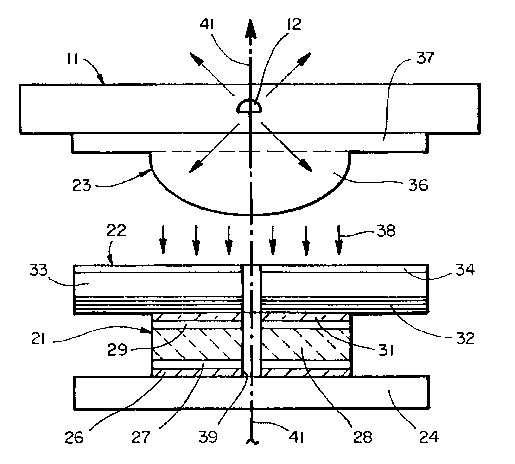
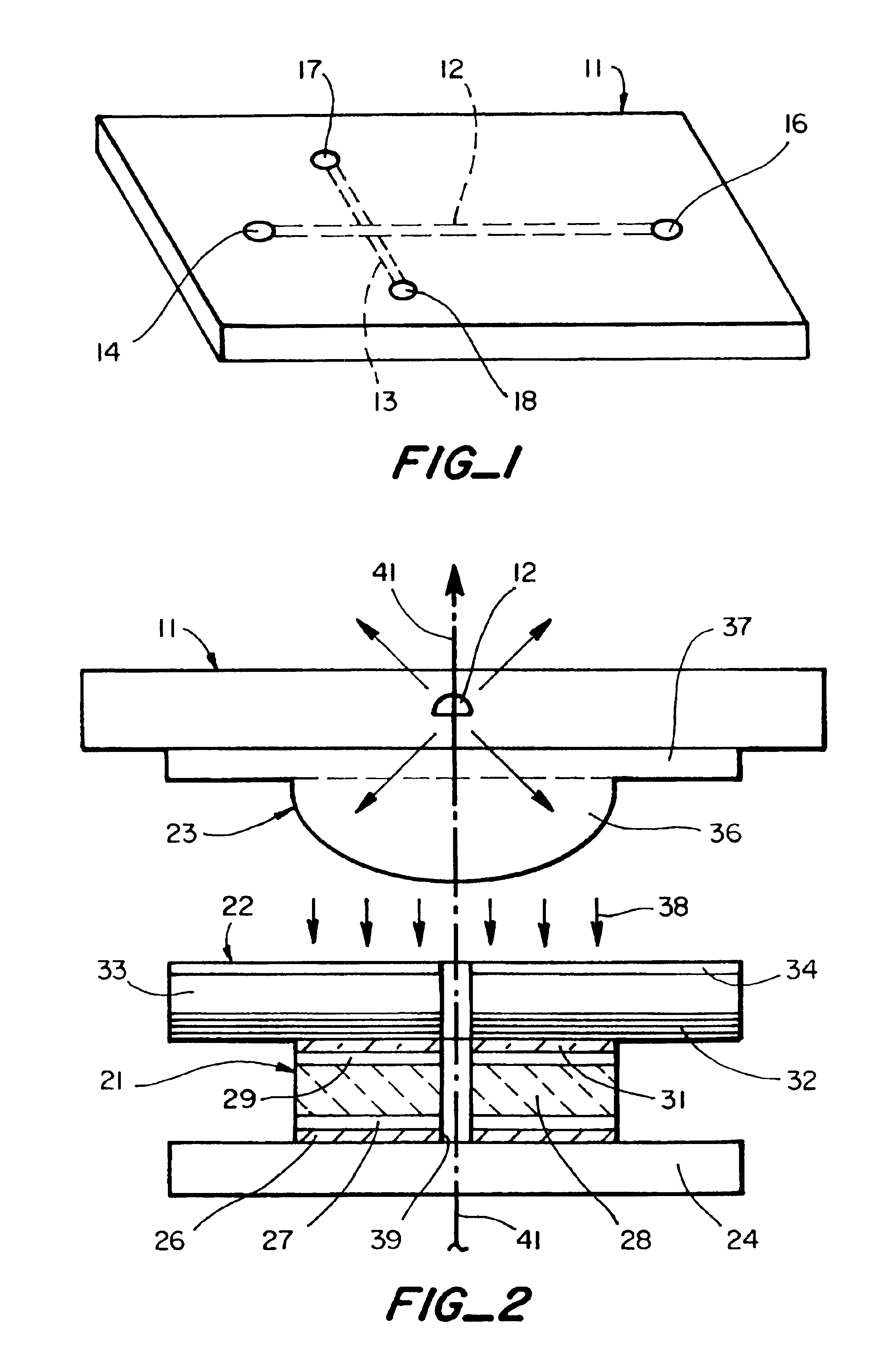
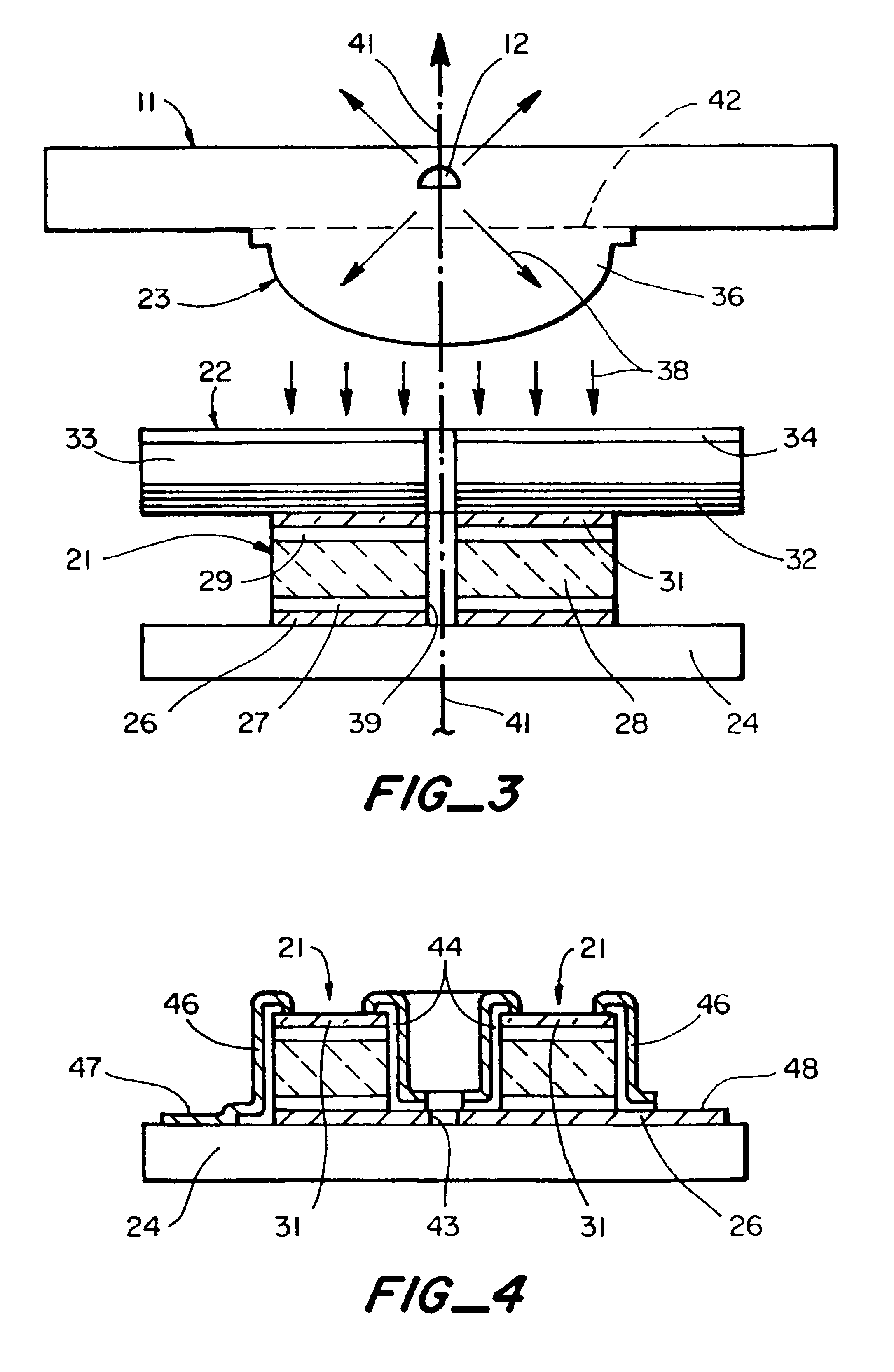
[0029]FIG. 1 schematically illustrates a capillary electrophoresis chip 11 with separation channel 12 and cross injection channel 13. Capillary electrophoresis separating voltage is applied between the cathode 14 and a...


PUM

PropertyMeasurementUnit
temperatureaaaaaaaaaa
deposition temperatureaaaaaaaaaa

Abstract

A miniaturized optical excitation and detector system is described for detecting fluorescently labeled analytes in electrophoretic microchips and microarrays. The system uses miniature integrated components, light collection, optical fluorescence filtering, and an amorphous a-Si:H detector for detection. The collection of light is accomplished with proximity gathering and / or a micro-lens system. Optical filtering is accomplished by integrated optical filters. Detection is accomplished utilizing a-Si:H detectors.

Description

RELATED APPLICATIONS[0002]This application claims priority to U.S. Provisional Application Ser. No. 60 / 385,770 filed Jun. 3, 2002.GOVERNMENT SUPPORT[0003]This invention was made with Government support under Grant No. FG03-91ER61125 awarded by the Department of Energy. The Government has certain rights to this invention.BRIEF DESCRIPTIONS OF THE INVENTION[0004]This invention relates generally to a solid state detector and optical system for detecting fluorescently labeled analytes in microchips and microarrays, and more particularly to a system employing a-Si:H photodetectors, filters and microlenses.BACKGROUND[0005]There is tremendous demand for chemical and bioanalytical devices that enable high throughput and performance assays in small point-of-care or point-of-analysis devices. Ultimately, these devices should be portable and disposable. To this end, microfabricated capillary array electrophoresis (μCAE) devices are a promising candidate. μCAE can be used to carry out a wide va...

Claims


Application Information

Patent Timeline
Patent Type & Authority Patents(United States)
IPC IPC(8): G01N21/64G01N21/25G01N27/447
CPCG01N21/255G01N21/6454G01N2021/6478G01J2003/104G01J2003/2806
Inventor MATHIES, RICHARD A.KAMEI, TOSHIHIROSCHERER, JAMES R.STREET, ROBERT A.
Owner PALO ALTO RES CENT INC
Why Eureka
Try Eureka