Stack chip module with electrical connection and adhesion of chips through a bump for improved heat release capacity

a technology of heat release capacity and chip, applied in the direction of semiconductor devices, semiconductor/solid-state device details, electrical apparatus, etc., can solve the problems of lowering the heat release capacity, difficult to obtain desired capacitance, and difficult process for fine line width and much development time, etc., to achieve the effect of improving the heat release capacity

Inactive Publication Date: 2005-03-15
SK HYNIX INC
View PDF17 Cites 32 Cited by
  • Summary
  • Abstract
  • Description
  • Claims
  • Application Information

AI Technical Summary

Benefits of technology

Therefore, the present invention has been made to solve the above problems and an object of the invention is to provide a stack chip module with improved heat release capacity.

Problems solved by technology

However, generally, one semiconductor chip is loaded in a package, making it difficult to obtain desired capacitance.
However, the method requires difficult processes for fine line width and much development time.
However, the conventional stack packages have difficulty in installing heat sink, thereby lowering capacity of heat release.
Furthermore, the electric signal paths of the upper package and that of the lower package are different relative to each other and therefore it is difficult to ensure electric reliability.
Moreover, junction of upper and lower packages is accomplished by solder joint of each outer lead and therefore it is also difficult to ensure solder joint reliability.
In the stack package according to the second method, the distance between upper and lower gold wires for signal transmission is so close that signal noise may be generated when the two chips are operated.
Moreover, it is impossible to rework the stack package.

Method used


Image

  • Stack chip module with electrical connection and adhesion of chips through a bump for improved heat release capacity
  • Stack chip module with electrical connection and adhesion of chips through a bump for improved heat release capacity
  • Stack chip module with electrical connection and adhesion of chips through a bump for improved heat release capacity

Examples


embodiment 1

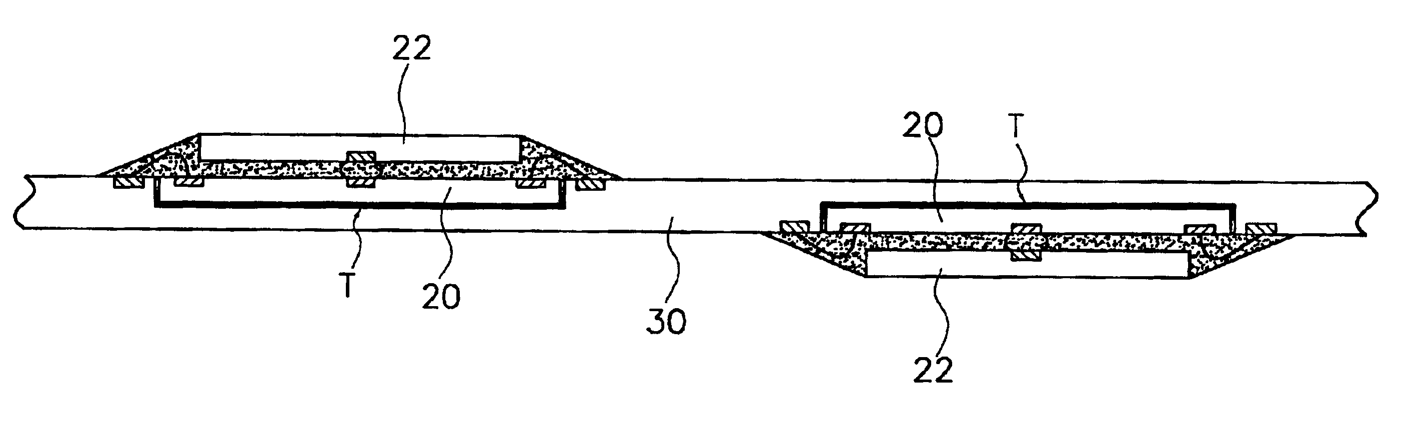
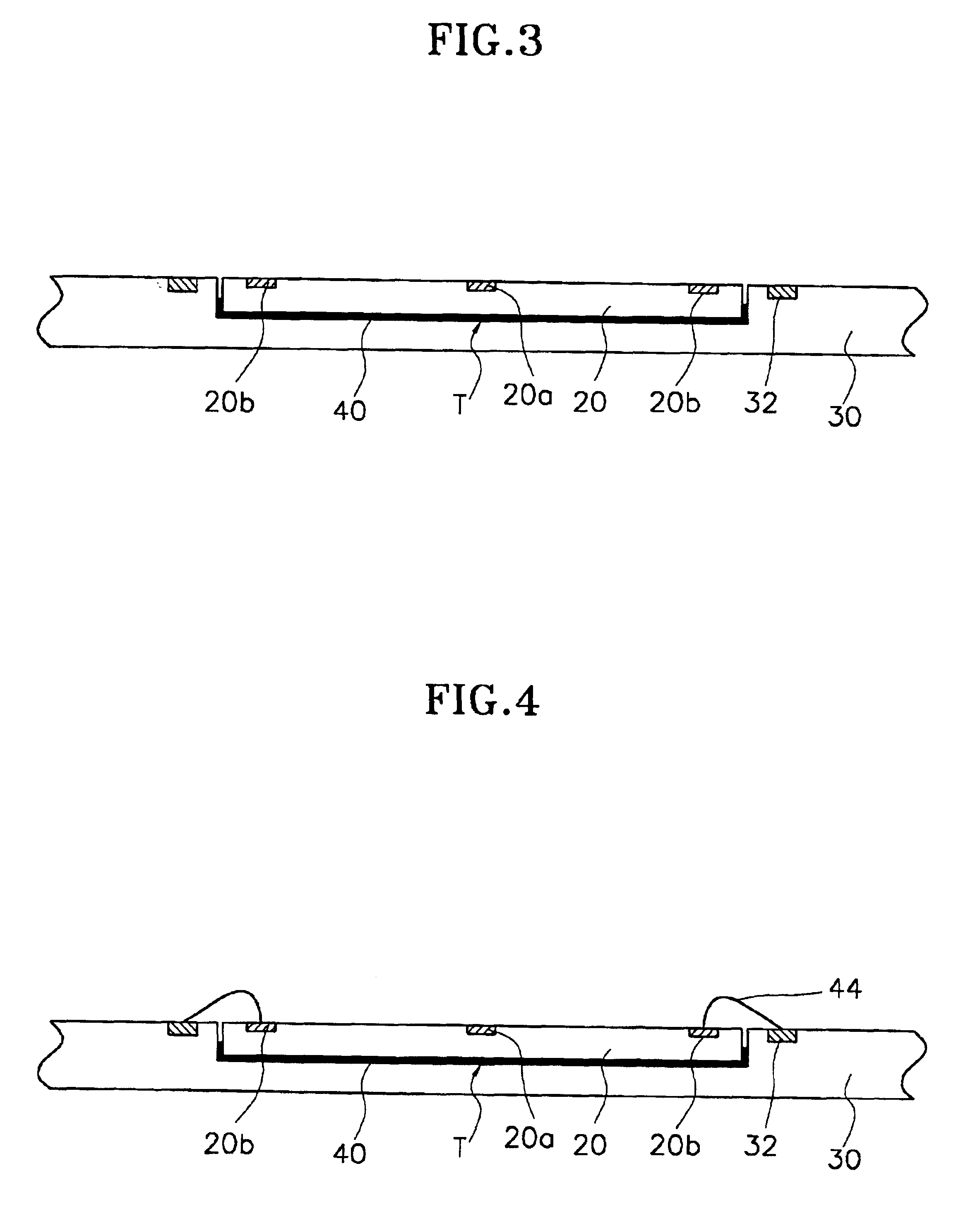
FIG. 6 is a cross sectional view showing a stack chip module according to a first embodiment of the present invention. As shown in FIG. 6, a lower semiconductor chip 20 (hereinafter referred to as the bottom chip) having a plurality of center pads 20a and a plurality of edge pads 20b is adhered in a groove T of a substrate 30 by adhesive 40 and the edge pad 20b is connected to the circuit pattern 32 by a gold wire 44. An upper semiconductor chip 22 (hereinafter referred to as the top chip) having a plurality of center pads 22a is arranged on the upper part of the bottom chip 20, the pad formative side being opposite to that of the bottom chip 20, wherein the center pad 22a of the top chip 22 and the center pad 20a of the bottom chip 20 are electrically connected by a bump 42. The wired bonded edge pad 20b of bottom chip 20 and a side of the top chip 22 including the circuit pattern 32 of substrate 30 are molded by a molding material 46.

In the bottom chip 20, edge pads 20b are electr...

embodiment 2

FIG. 7 is a cross sectional view showing a stack chip module according to a second embodiment of the present invention. Referring to FIG. 7, the first heat sink 50 is adhered on a back side of exposed top chip 22. Therefore, the stack chip module according to the second embodiment of the present invention has improved heat release capacity.

embodiment 3

FIG. 8 is a cross sectional view showing a stack chip module according to a third embodiment of the present invention. Referring to FIG. 8, a second heat sink 52 is prepared on a substrate whereon a bottom chip 20 is installed, that is, on a bottom of groove T, to be exposed to the other side of the substrate 30. The second heat sink 52 is desirably formed by a plating process in manufacturing the substrate 30 and the upper side thereof corresponds to the bottom of groove T, thereby being in contact with the bottom chip 20.

Although it is not shown in the drawings, a second heat sink 50 may be additionally adhered on the back side of the exposed top chip 22 in order to improve heat release capacity.


PUM


Abstract

A stack chip module includes a substrate having a predetermined-size groove on one side and a circuit pattern, one end of the circuit pattern being adjacent to the groove; a first semiconductor chip adhered in the groove of the substrate by adhesive and having a plurality of center pads and a plurality of edge pads, electrically connected to each other, on the upper part thereof; a plurality of gold wires for electrically connecting the circuit pattern of the substrate and the edge pads of the first semiconductor chip, respectively; a second semiconductor chip having a plurality of center pads corresponding to those of the first semiconductor chip, the formative side being opposite to that of the first semiconductor chip; and a plurality of bumps interposed between the center pads of the first semiconductor chip and the center pads of the second semiconductor chip for joining and electrically connecting them.

Description

BACKGROUND OF THE INVENTION1. Field of the InventionThe present invention relates to semiconductor devices and, more particularly, to a stack chip module improving heat release properties and electric and mechanical reliability.2. Description of the Related ArtAs high-performance electric appliances are developed, efforts are focused on research to mount a large number of packages on a limited substrate. However, generally, one semiconductor chip is loaded in a package, making it difficult to obtain desired capacitance.A method has been proposed in which a large number of cells are fabricated in a limited area in order to increase capacitance of a memory chip, that is, to accomplish high integration. However, the method requires difficult processes for fine line width and much development time. Therefore, a stacking method has been developed in order to accomplish high integration with ease.The stacking method increases memory capacitance by stacking two or more semiconductor chips....

Claims


Application Information

Patent Timeline
Patent Type & Authority Patents(United States)
IPC IPC(8): H01L21/56H01L25/065H01L21/02H01L23/36H01L23/34H01L25/18H01L23/12H01L25/07
CPCH01L21/563H01L23/36H01L24/32H01L24/29H01L25/0652H01L25/0657H01L2224/45144H01L2224/32245H01L24/48H01L2924/01033H01L2224/73215H01L2224/73204H01L2924/30105H01L2924/15165H01L2924/15153H01L2224/16145H01L2224/48091H01L2224/48247H01L2224/4826H01L2224/73203H01L2224/73207H01L2224/73253H01L2224/73265H01L2224/83102H01L2224/92125H01L2225/0651H01L2225/06513H01L2225/06572H01L2225/06582H01L2225/06589H01L2924/01004H01L2924/01005H01L2924/01078H01L2924/01079H01L2924/01082H01L2924/00014H01L2924/00H01L2924/00012H01L2924/181H01L2924/12042H01L2224/05571H01L2224/05573H01L24/45H01L2224/45015H01L2924/207H01L23/12
Inventor HONG, JOON KI
Owner SK HYNIX INC
Why Eureka
Try Eureka