Interconnect substrate, semiconductor device, methods of fabricating, inspecting, and mounting the semiconductor device, circuit board, and electronic instrument

a technology of interconnecting substrates and semiconductor devices, which is applied in the direction of solid-state devices, basic electric elements, printed circuit non-printed electric components association, etc., can solve the problems of difficult to bend and superpose a substrate accurately at a desired position, and difficult to bond a plurality of substrates at a precise position, so as to achieve the effect of easy mounting

Inactive Publication Date: 2005-03-15
SEIKO EPSON CORP
View PDF42 Cites 63 Cited by
  • Summary
  • Abstract
  • Description
  • Claims
  • Application Information

AI Technical Summary

Benefits of technology

Since the first and second portions are separated, the substrate can be easily bent or folded in the region between the first and second portions.
According to this configuration, the relative positions between the end part as a positioning reference in the first portion and the external terminals are fixed, therefore the positioning of the external terminals can be easily done by using the end part as a positioning reference. If the electrical characteristics of the semiconductor device are inspected, it is sufficient to put the semiconductor device into a socket. Moreover, rate of defectives due to mispositioning of the external terminals can be reduced when mounting the semiconductor device on a circuit board.
According to the present invention, the positioning for the mounting can be easily done by using the end parts of the first portion as the positioning references.

Problems solved by technology

However, it is difficult to bend and superpose a substrate accurately at a desired position.
It is also difficult to bond a plurality of substrates at a precise position.

Method used


Image

  • Interconnect substrate, semiconductor device, methods of fabricating, inspecting, and mounting the semiconductor device, circuit board, and electronic instrument
  • Interconnect substrate, semiconductor device, methods of fabricating, inspecting, and mounting the semiconductor device, circuit board, and electronic instrument
  • Interconnect substrate, semiconductor device, methods of fabricating, inspecting, and mounting the semiconductor device, circuit board, and electronic instrument

Examples


first embodiment

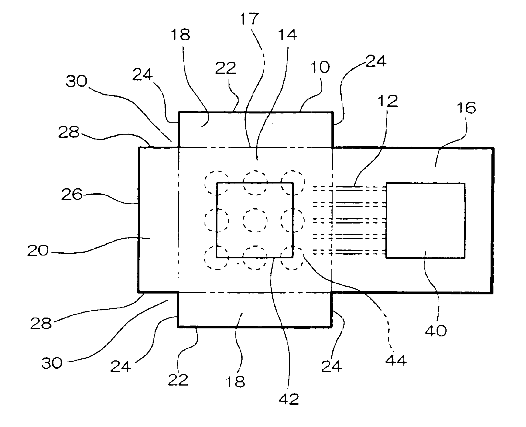
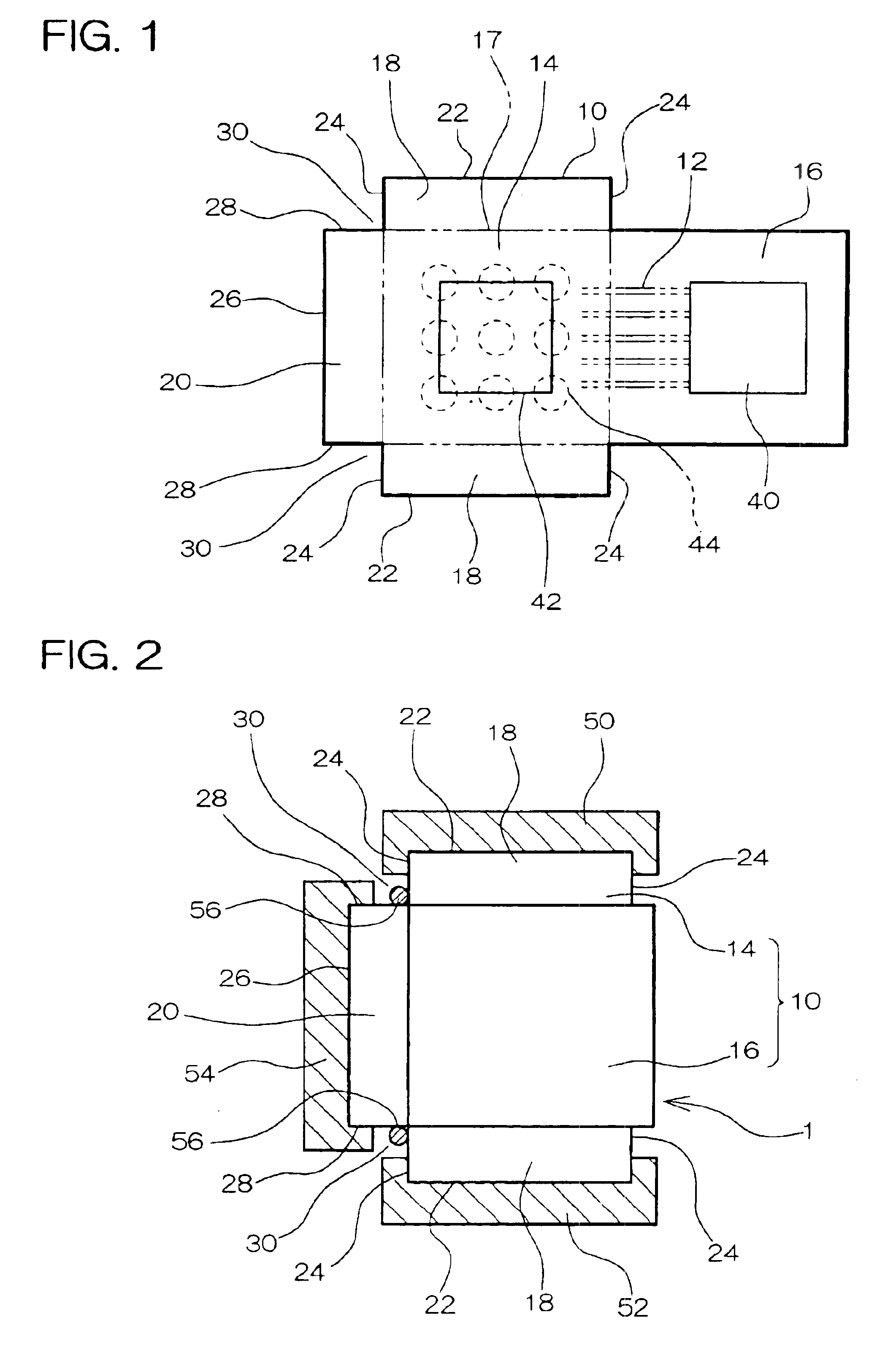
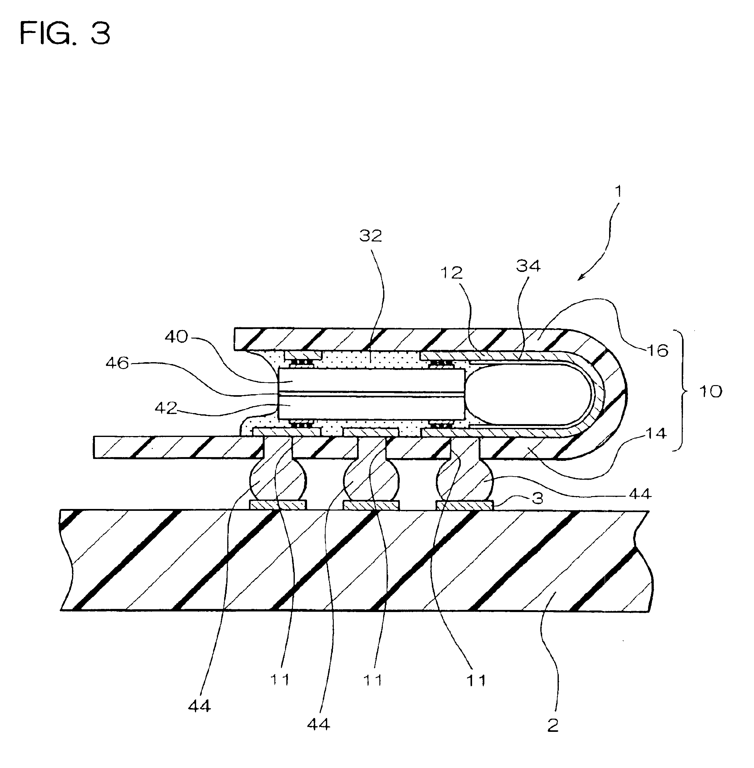
FIG. 1 is a view illustrating a method of fabricating a semiconductor device according to a first embodiment to which the present invention is applied. FIG. 2 is a view illustrating a semiconductor device according to the present embodiment and a method for inspecting or mounting the semiconductor device. FIG. 3 is a view showing a circuit board equipped with the semiconductor device according to the present embodiment.

Substrate

A substrate 10 shown in FIG. 1 is used in the semiconductor device according to the present embodiment. The substrate 10 is used as an interposer for mounting at least one (plurality in FIG. 1) of semiconductor chips 40 and 42. The material for the substrate 10 may be any organic or inorganic material or a composite structure of these materials. As examples of the substrate 10 formed using an organic material, a two-layer or three-layer flexible substrate formed of a polyimide resin and the like can be given. It is preferable to use a flexible substrate in th...

second embodiment

FIG. 4 is a view illustrating a method of fabricating a semiconductor device according to a second embodiment to which the present invention is applied. FIG. 5 is a view illustrating a semiconductor device according to the present embodiment and a method for inspecting or mounting the semiconductor device. FIG. 6 is a view illustrating a method of fabricating a semiconductor device according to a modification example of the present embodiment.

In the present embodiment, a substrate 60 shown in FIG. 4 is used. Interconnect pattern 62 is formed on the substrate 60. The substrate 60 has first and second portions 64 and 66. The first and second portions 64 and 66 are formed separately but connected by the interconnect pattern 62. The interconnect pattern 62 is preferably insulated by applying flexible resist thereon.

The first portion 64 has a projected section 68 which extends from one edge (virtual edge) of a rectangular body section in a direction perpendicular thereto and has a width ...

third embodiment

FIG. 7 is a view showing a semiconductor device according to a third embodiment to which the present invention is applied. This semiconductor device includes a substrate 90 having first and second portions 92 and 94. The first and second portions 92 and 94 are stacked. The first and second portions 92 and 94 may be formed either continuously and integrally or separately. The details thereof are described in the first and second embodiments. At least one semiconductor chip (not shown) is provided between the first and second portions 92 and 94. External terminals (not shown) may be provided on the first portion 92.

In the present embodiment, a plurality of holes 96 is formed on the first portion 92. A plurality of end parts for forming the holes 96 becomes the positioning references of the semiconductor device. Specifically, the semiconductor device can be easily positioned by inserting pins or the like into the holes 96.

The second portion 94 is designed so that the second portion 94 ...


PUM


Abstract

A semiconductor device including a substrate (10). An interconnect pattern (12) is formed over the substrate (10), and the substrate (10) has a first portion (14) and a second portion (16) to be superposed on the first portion (14). The first portion (14) has edges (22), (24), (26) and (28) as positioning references. The second portion (16) has a shape to be superposed over the first portion (14) except the edges (22), (24), (26) and (28).

Description

TECHNICAL FIELDThe present invention relates to an interconnect substrate, a semiconductor device, methods of fabricating, inspecting, and mounting the semiconductor device, a circuit board, and an electronic instrument.BACKGROUND ARTPackages having a structure in which a first portion of a substrate equipped with a semiconductor chip is bent and bonded to a second portion of the substrate provided with external terminals, or in which a first substrate equipped with a semiconductor chip is bonded to a second substrate provided with the external terminals have been developed. Since these packages enable the area of the substrate to be increased while reducing the planar size, the degree of freedom relating to the design of the interconnect pattern increases. Therefore, a stacked structure in which a number of semiconductor chips are superposed one on top of the other can be easily formed.However, it is difficult to bend and superpose a substrate accurately at a desired position. It i...

Claims


Application Information

Patent Timeline
Patent Type & Authority Patents(United States)
IPC IPC(8): H01L23/52H01L23/544H01L23/538H01L23/498H01L23/48H05K1/18H05K1/14
CPCH01L23/49816H01L23/5387H01L23/544H01L2924/07811H01L2224/73253H01L2224/73204H01L2224/32225H01L2224/32145H01L2223/54473H01L2924/01078H01L2924/01079H01L2924/09701H05K1/141H05K1/189H01L2224/16225H01L2924/00012H01L2924/00H01L2224/05573H01L2224/05568H01L2924/00014H01L2224/05599H01L23/12
Inventor HASHIMOTO, NOBUAKI
Owner SEIKO EPSON CORP
Why Eureka
Try Eureka