Manufacturing method for semiconductor substrate, and semiconductor device having a strained Si layer

Inactive Publication Date: 2005-03-22
SHARP KK
View PDF6 Cites 4 Cited by
  • Summary
  • Abstract
  • Description
  • Claims
  • Application Information

AI Technical Summary

Benefits of technology

The present invention is provided in view of the above described problems and a purpose thereof is to provide a method for manufacturing a semiconductor substrate having a strained Si/SiGe/Si structure wherein the strained SiGe film in the

Problems solved by technology

That is to say, defects due to this residual oxygen cause deterioration in the crystallinity of the

Method used


Image

  • Manufacturing method for semiconductor substrate, and semiconductor device having a strained Si layer
  • Manufacturing method for semiconductor substrate, and semiconductor device having a strained Si layer
  • Manufacturing method for semiconductor substrate, and semiconductor device having a strained Si layer

Examples


Embodiment Construction

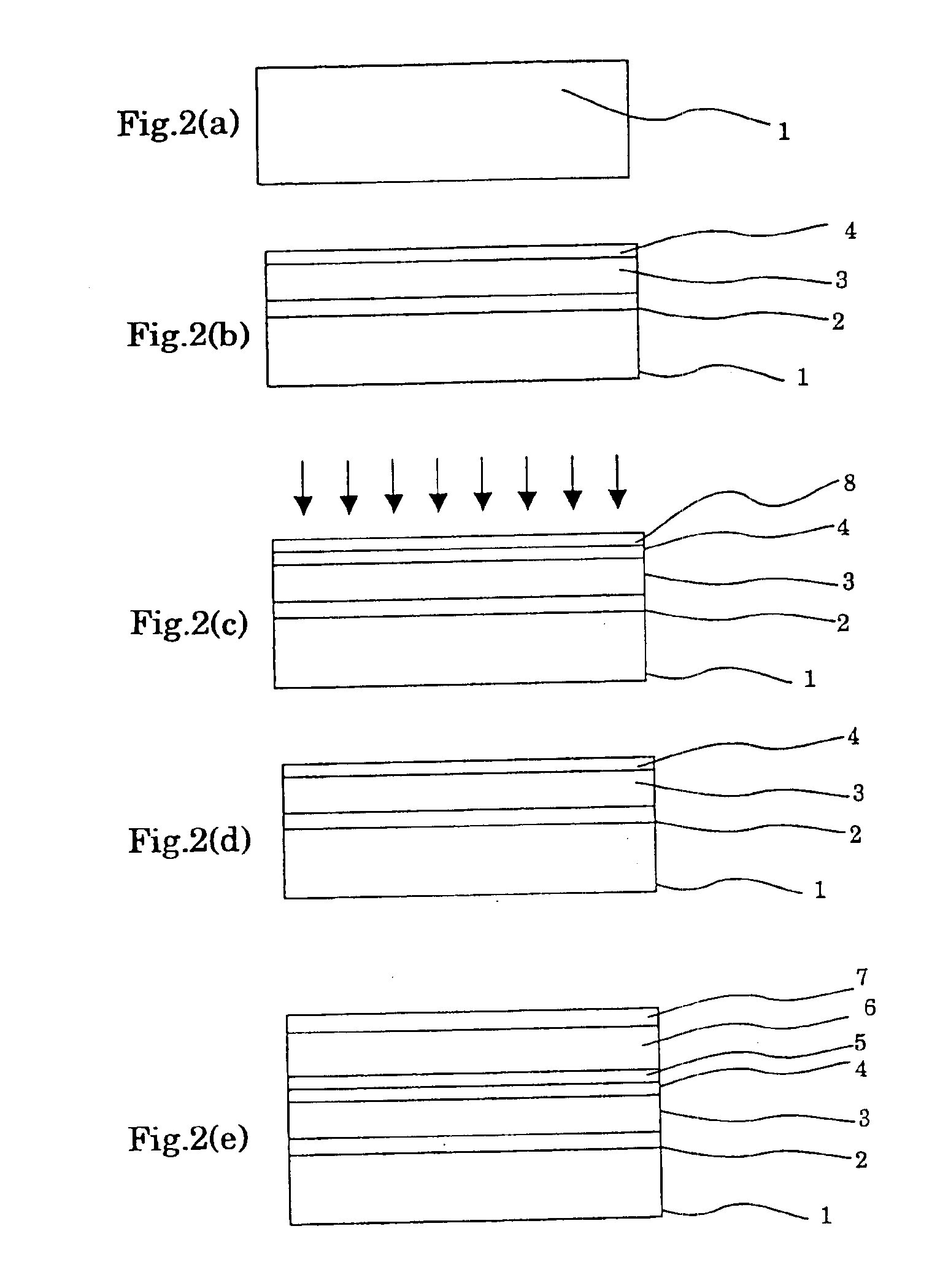
According to the method for manufacturing a semiconductor substrate of the present invention, first, a first buffer Si layer, a first strained SiGe layer and a first Si layer are formed above a substrate having a silicon surface. Here, the substrate having a silicon surface may be a so-called SOI, SOS substrate, or the like, which have a monocrystal silicon layer on the surface, or a monocrystal silicon substrate. It is preferable for the substrate to be used after removal of the natural oxide film on the surface as a result of a washing step. Any method known in the art can be applied in the washing step. A variety of methods, such as boiling with sulfuric acid, RCA washing and / or acid washing using fluoric acid, for example, can be cited.

The first buffer Si layer, the first strained SiGe layer and the first Si layer can be formed according to a variety of known methods such as, for example, a CVD method, a sputtering method, a vapor deposition method or an MEB method. In particula...


PUM


Abstract

The present invention provides a method for manufacturing a semiconductor substrate, comprising the step of: forming a first buffer Si layer on a substrate having a silicon surface; epitaxially growing, in sequence, a first strained SiGe layer and a first Si layer above the first buffer Si layer; implanting ions into the resulting substrate followed by annealing so as to relax the lattice of the first strained SiGe layer and to thereby providing tensile strain in the first Si layer and so that tensile strain is provided in the first Si layer; and epitaxially growing, in sequence, a second buffer Si layer and a second SiGe layer above the resulting substrate; and forming a second Si layer having tensile strain on the second SiGe layer.

Description

CROSS-REFERENCE TO RELATED APPLICATIONThis application is related to Japanese application No. 2002-263158 filed on Sep. 9, 2002, whose priority is claimed under 35 USC § 119, the disclosure of which is incorporated by reference in its entirety.BACKGROUND OF THE INVENTION1. Field of the InventionThe present invention relates to a manufacturing method for a semiconductor substrate, a semiconductor substrate and a semiconductor device, in particular relates to a manufacturing method for a semiconductor substrate having a strained Si layer, a semiconductor substrate having a strained Si layer and a semiconductor device having a strained Si layer.2. Description of Related ArtIncreasing the mobility of electrons and holes that move in a semiconductor element is an effective means for enhancing the performance of a semiconductor device.In a semiconductor device formed in a substrate made of silicon monocrystal, however, the upper limit of mobility of electrons that move in the silicon mono...

Claims


Application Information

Patent Timeline
IPC IPC(8): H01L21/265H01L21/337H01L21/02H01L21/26H01L29/66H01L29/02H01L29/10H01L29/80H01L29/161H01L21/20H01L21/336H01L29/78H01L29/786
CPCH01L21/2605H01L21/26506H01L29/66916H01L29/802H01L29/1054Y10S438/933
Inventor TAKENAKA, MASAHIRO
Owner SHARP KK
Why Eureka
Try Eureka