Eureka AIR delivers breakthrough ideas for toughest innovation challenges, trusted by R&D personnel around the world.

Crystalline silicon solar cell without Ag main grid line and manufacturing process therefor

A technology for solar cells and manufacturing processes, applied in sustainable manufacturing/processing, circuits, photovoltaic power generation, etc., can solve problems such as failure to solve the problem of single-cell battery testing, enhance the passivation of aluminum back field, and improve conversion efficiency , the effect of low production cost

Inactive Publication Date: 2016-04-13
HENGDIAN GRP DMEGC MAGNETICS CO LTD
View PDF4 Cites 2 Cited by
  • Summary
  • Abstract
  • Description
  • Claims
  • Application Information

AI Technical Summary

Problems solved by technology

However, the biggest flaw of this design is that it fails to solve the problem of single-chip battery testing, because the module packaging requires batteries of the same conversion efficiency gear to be packaged into a power generation unit

Method used


Image

  • Crystalline silicon solar cell without Ag main grid line and manufacturing process therefor
  • Crystalline silicon solar cell without Ag main grid line and manufacturing process therefor

Examples


Embodiment 1

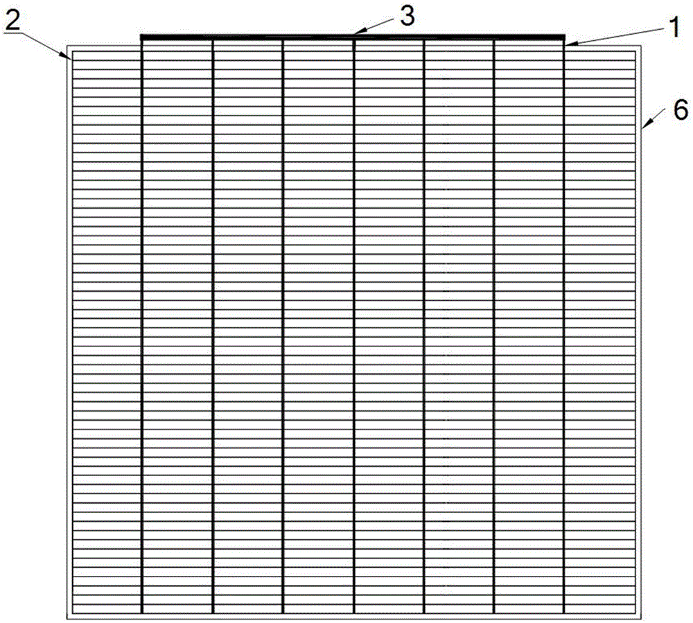
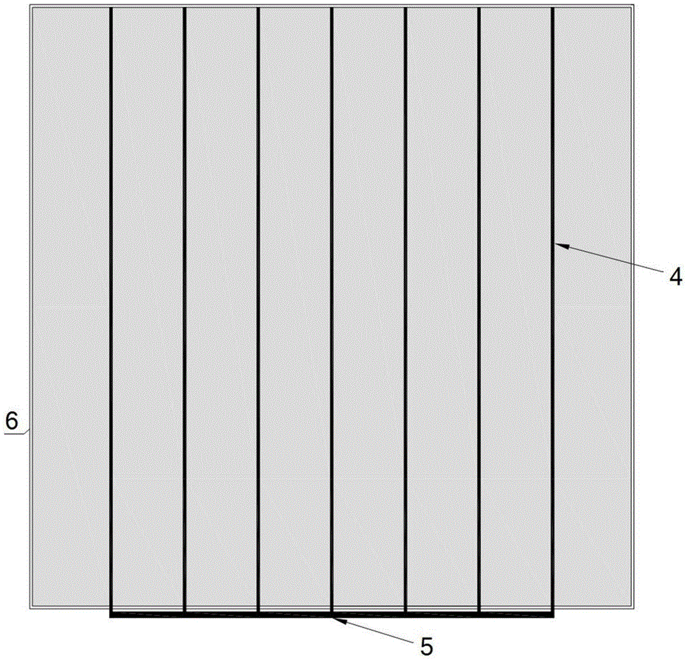
[0039] According to the trial production process of P-type polycrystalline batteries, the batteries only need to be printed and sintered by the back electric field and the front Ag sub-gate electrode, and a batch of P-type 156mm polycrystalline batteries without busbars are trial-produced, and a batch of traditional battery control groups are set; first press According to the technical solution described in the content of the present invention, 7 busbar lines of copper-tin solder strips with a width of 0.7mm and 3mm beyond the battery are evenly fixed on the front and back sides of the battery without busbar; It is a 1.5mm copper-tin ribbon, which is used for battery test contact wires and battery connection wires during component packaging; then the fixed copper-tin ribbon main grid polycrystalline battery is cured in an oven at 140°C 25s, forming an Ag-free busbar polycrystalline cell. Finally, compare the efficiency, electrical performance and other data of the Ag-free busb...

Embodiment 2

[0041] According to the trial production process of P-type monocrystalline cells, the cells only need to be printed and sintered in the back electric field and the front Ag sub-gate electrode, and a batch of P-type 156mm single crystal cells without busbars are trial-produced, and a batch of traditional battery control groups are set up; first press In the technical solution described in the content of the present invention, 7 busbar lines of copper-tin soldering strips with a width of 0.7mm and 3mm beyond the battery are evenly fixed on the front and back sides of the battery without busbar; Copper-tin solder strip with a width of 1.5mm is used for battery test contact wires and battery connection wires during component packaging; then place the fixed copper-tin solder strip main grid polycrystalline battery in an oven at 140°C Curing for 25s to form an Ag-free busbar polycrystalline cell. Finally, compare the efficiency, electrical performance and other data of the Ag-free b...

Embodiment 3

[0043] According to the trial production process of N-type monocrystalline double-sided batteries, the batteries only need to be printed and sintered with Ag sub-gate electrodes on the back and front, and a batch of N-type 156mm single-crystalline double-sided batteries without busbars will be trial-produced, and a batch of traditional battery control groups will be set up. ; First, according to the technical scheme described in the contents of the present invention, evenly fix 7 copper-tin solder strip busbar lines with a width of 0.7mm and 3mm beyond the battery part on the front and back sides of the battery without busbar; secondly, on the busbar Weld the copper-tin ribbon with a grid width of 1.5mm at the terminal point, which is used for the battery test contact wire and the battery connection wire during component packaging; then place the polycrystalline battery with the fixed copper-tin ribbon main grid at 140°C Cured in an oven for 25s to form Ag-free busbar polycryst...


PUM


Abstract

The invention discloses a crystalline silicon solar cell without an Ag main grid line and a manufacturing process therefor. The crystalline silicon solar cell comprises a solar cell body, wherein the solar cell body comprises a light-receiving surface and a backlight surface; multiple light-receiving surface main grid lines and multiple light-receiving surface secondary grid lines are arranged on the light-receiving surface of the solar cell body; the light-receiving surface main grid lines and the light-receiving surface secondary grid lines are arranged in a perpendicular manner mutually; multiple backlight surface main grid lines are arranged on the backlight surface of the solar cell body; the light-receiving surface main grid lines and the backlight surface main grid lines are all manufactured by first conductive solder strips; and the light-receiving surface secondary grid lines are Ag secondary grid lines. The crystalline silicon solar cell without the Ag main grid line and the manufacturing process therefor have the beneficial effects that the Ag slurry consumption is greatly reduced, the cost is lowered, a sintering area between Ag and silicon is reduced, the defect concentration is lowered, and the conversion efficiency is improved; multiple main grid lines can be designed, so that the battery conversion efficiency is further improved; and quantity production can be realized, and the production cost is low.

Description

technical field [0001] The invention relates to the related technical field of crystalline silicon solar cells, in particular to an Ag-free busbar crystalline silicon solar cell and a manufacturing process thereof. Background technique [0002] Since the development of photovoltaics, crystalline silicon solar cells have become the main product in the market. In recent years, the cost of crystalline silicon solar cells has been decreasing, and the cost of photovoltaic power generation has also been accepted by people in large-scale applications. The cost of crystalline silicon solar cells mainly consists of two parts: silicon wafer cost and battery manufacturing cost. The traditional crystalline silicon solar cell manufacturing process mainly includes cleaning and making texture, diffusion making PN junction, etching / removing phosphorus silicon glass, PECVD anti-reflection coating, screen printing electrode, and sintering test. , the largest manufacturing cost is the cost o...

Claims


Application Information

Patent Timeline
Patent Type & Authority Applications(China)
IPC IPC(8): H01L31/068H01L31/0224H01L31/05H01L31/18
CPCH01L31/022433H01L31/0504H01L31/068H01L31/1804Y02E10/547Y02P70/50
Inventor 陈金灯董方李虎明
Owner HENGDIAN GRP DMEGC MAGNETICS CO LTD
Why Eureka
Eureka Blog
Learn More