Surge protection semiconductor device

a surge protection and semiconductor technology, applied in the direction of overvoltage protection resistors, emergency protective arrangements for limiting excess voltage/current, and arrangements responsive to excess voltage, etc., can solve the problems of increasing product size, complicated mounting process, and high cost of products

Inactive Publication Date: 2005-03-22
SHINDENGEN ELECTRIC MFG CO LTD
View PDF14 Cites 72 Cited by
  • Summary
  • Abstract
  • Description
  • Claims
  • Application Information

AI Technical Summary

Benefits of technology

FIG. 5 is a view for explaining the circuit of a surge prote...

Problems solved by technology

This complicates the mounting process, increases the product size, and makes the product expensive.
Unfortunately, this technique is applicable only to a circuit configuration, as shown in FIG. 5, in which a pn...

Method used


Image

  • Surge protection semiconductor device
  • Surge protection semiconductor device
  • Surge protection semiconductor device

Examples


second embodiment

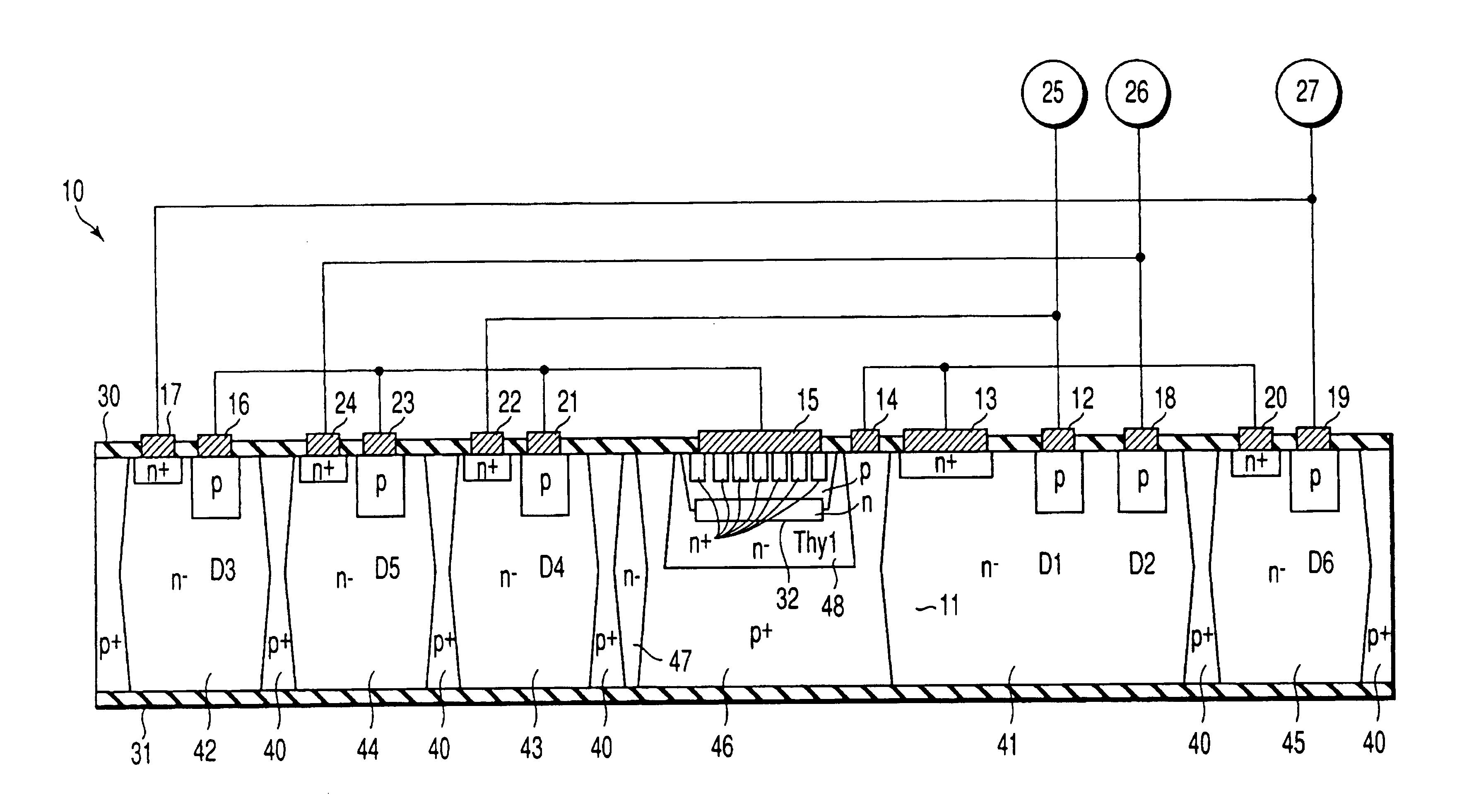
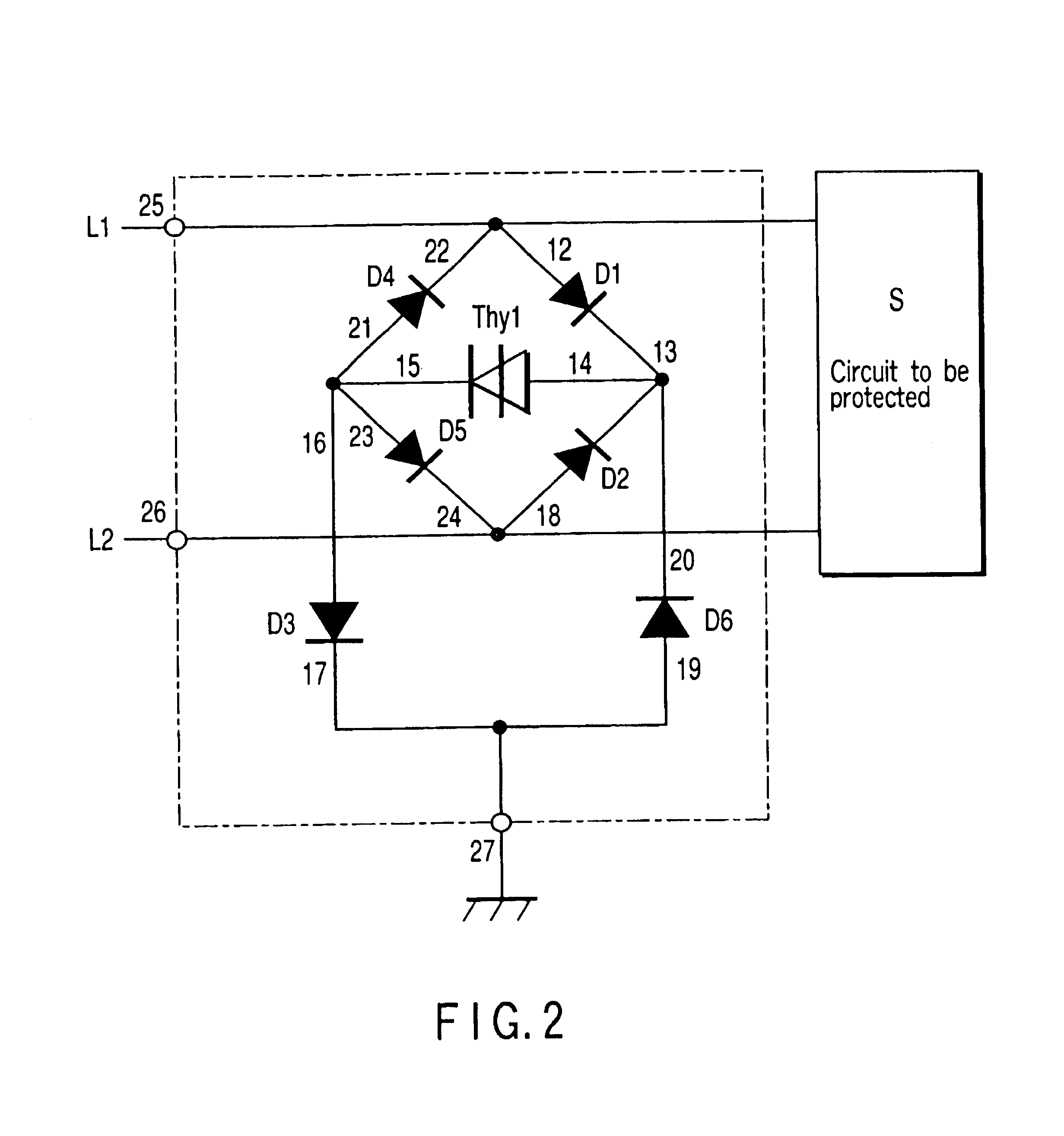
FIG. 3 is a sectional view showing a surge protection semiconductor device according to the present invention. In FIG. 3, the same reference numerals as in FIG. 1 denote the same parts.

A thyristor element Thy1 and first, second, and sixth diode elements D1, D2, and D6 are provided as a vertical element structure in consideration of the surge withstand voltage and the like. The remainder of the structure is the same as in FIG. 1.

In this structure, it is also possible to omit the isolation region 40 between an element region 41 forming the diode elements D1 and D2 and an element region 45 forming D6.

In this embodiment, the thyristor element Thy1 and first, second, and sixth diode elements D1, D2, and D6 are provided as the vertical element structure, thus obtaining a surge protection semiconductor device having an increased surge withstand voltage.

third embodiment

FIG. 4 is a sectional view showing a surge protection semiconductor device according to the present invention. In FIG. 4, the same reference numerals as in FIG. 1 denote the same parts.

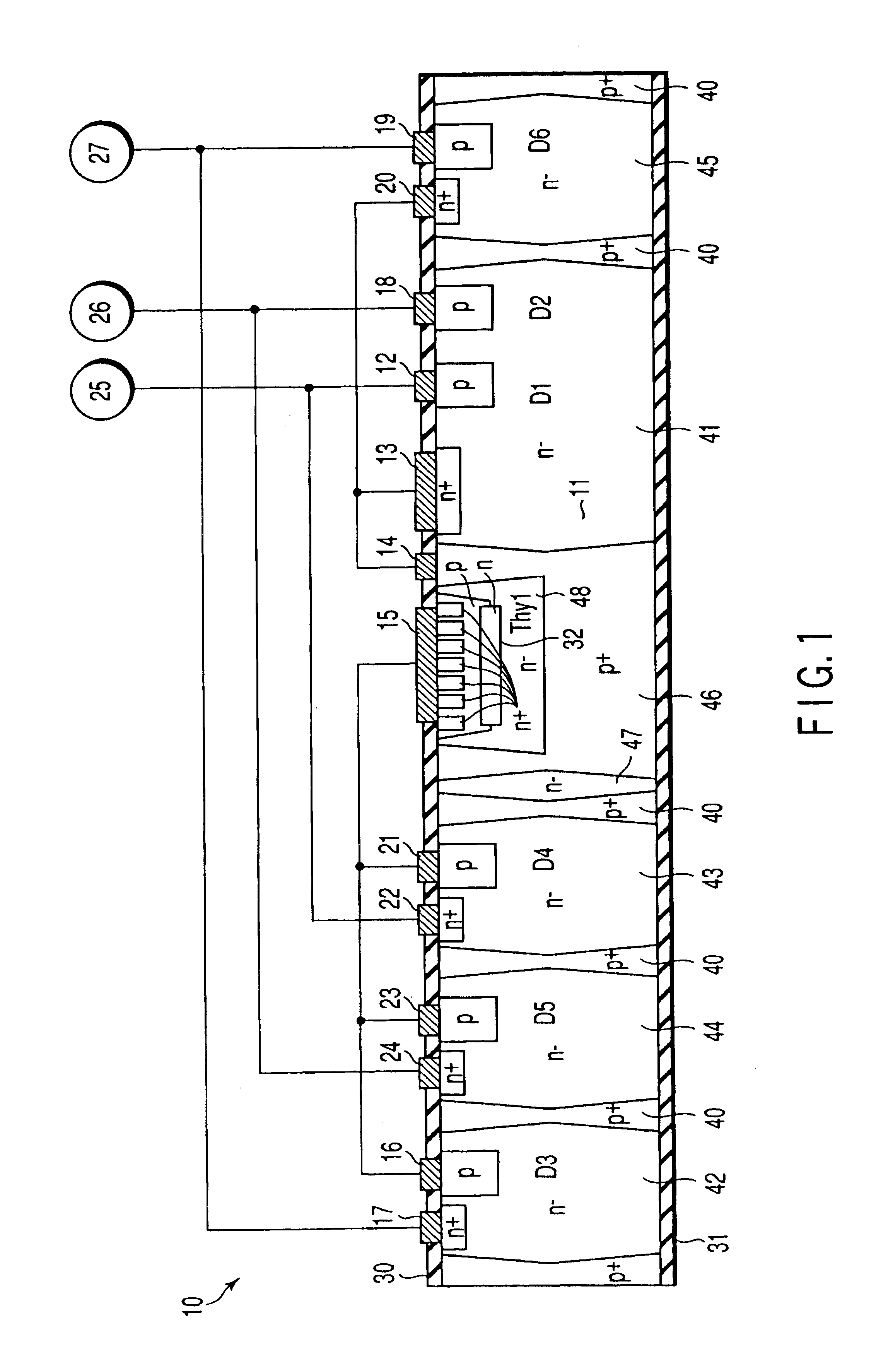
A thyristor element Thy1 and first to sixth diode elements D1 to D6 are provided as a vertical element structure in consideration of the surge withstand voltage and the like. In this structure, an n−-type semiconductor substrate 11 is separated by a p+-type isolation region 40 to provide an n−-type element region 50 for forming the thyristor element Thy1 and an n−-type element region 51 for forming the first, second, and sixth diode elements D1, D2, and D6.

The element region 50 includes an anode region formed from the second surface, an n-type buried layer 32 formed from the first surface and having an impurity concentration higher than that of the semiconductor substrate, a p-type base region, and a plurality of n+-type emitter layers.

The element region 51 includes anode regions of the first, second,...


PUM


Abstract

A pnpn thyristor element Thy1 and six pn diode elements D1, D2, D3, D4, D5, and D6 are formed in a semiconductor substrate of a first conductivity type, and separated into six regions by a diffusion layer of a second conductivity type which also functions as the anode of the thyristor element Thy1. A double isolation diffusion layer is disposed between the region of the thyristor element Thy1 and three pn diode elements D1 ·D2 and D6, and the region of the three remaining pn diodes D3, D4, and D5. Surface connection is performed to provide a balance type surge protection circuit.

Description

BACKGROUND OF THE INVENTION1. Field of the InventionThe present invention relates to a semiconductor surge protection device for protecting circuit systems in communication apparatuses, computers, and the like from an overvoltage and overcurrent such as lightning surge and switching surge.2. Description of the Related ArtSurge protection devices of this type have been achieved by combining pnpn thyristor elements and pn diode elements on a substrate to provide a desired circuit. These techniques are disclosed in U.S. Pat. Nos. 6,104,591, 5,512,784, and 4,644,437.In a surge protection device having the above arrangement, however, a plurality of parts, i.e., pnpn surge protection elements and pn diode elements are mounted on a substrate. This complicates the mounting process, increases the product size, and makes the product expensive.Also, the conventional technique comprising a monolithic structure of pnpn thyristor elements and pn diode elements is disclosed in U.S. Pat. No. 6,075,...

Claims


Application Information

Patent Timeline
IPC IPC(8): H01L29/74H01L29/66H01L27/08H01L27/02
CPCH01L27/0251H01L29/74H01L27/0817H01L27/0814
Inventor OKA, RITSUO
Owner SHINDENGEN ELECTRIC MFG CO LTD
Why Eureka
Try Eureka