Semiconductor device having a thin-film circuit element provided above an integrated circuit

a technology of thin-film circuit elements and semiconductor devices, applied in the direction of semiconductor devices, semiconductor/solid-state device details, electrical devices, etc., can solve the problem of serious design limitations

Inactive Publication Date: 2005-03-22
CASIO COMPUTER CO LTD
View PDF29 Cites 36 Cited by
  • Summary
  • Abstract
  • Description
  • Claims
  • Application Information

AI Technical Summary

Benefits of technology

The object of the present invention is to provide a semiconductor device, such as a CSP, having a re-wiring provided over a circuit element formation region of a semiconducto

Problems solved by technology

Because of this, the re-wiring segments 7 cannot freely be arrang

Method used


Image

  • Semiconductor device having a thin-film circuit element provided above an integrated circuit
  • Semiconductor device having a thin-film circuit element provided above an integrated circuit
  • Semiconductor device having a thin-film circuit element provided above an integrated circuit

Examples


first embodiment

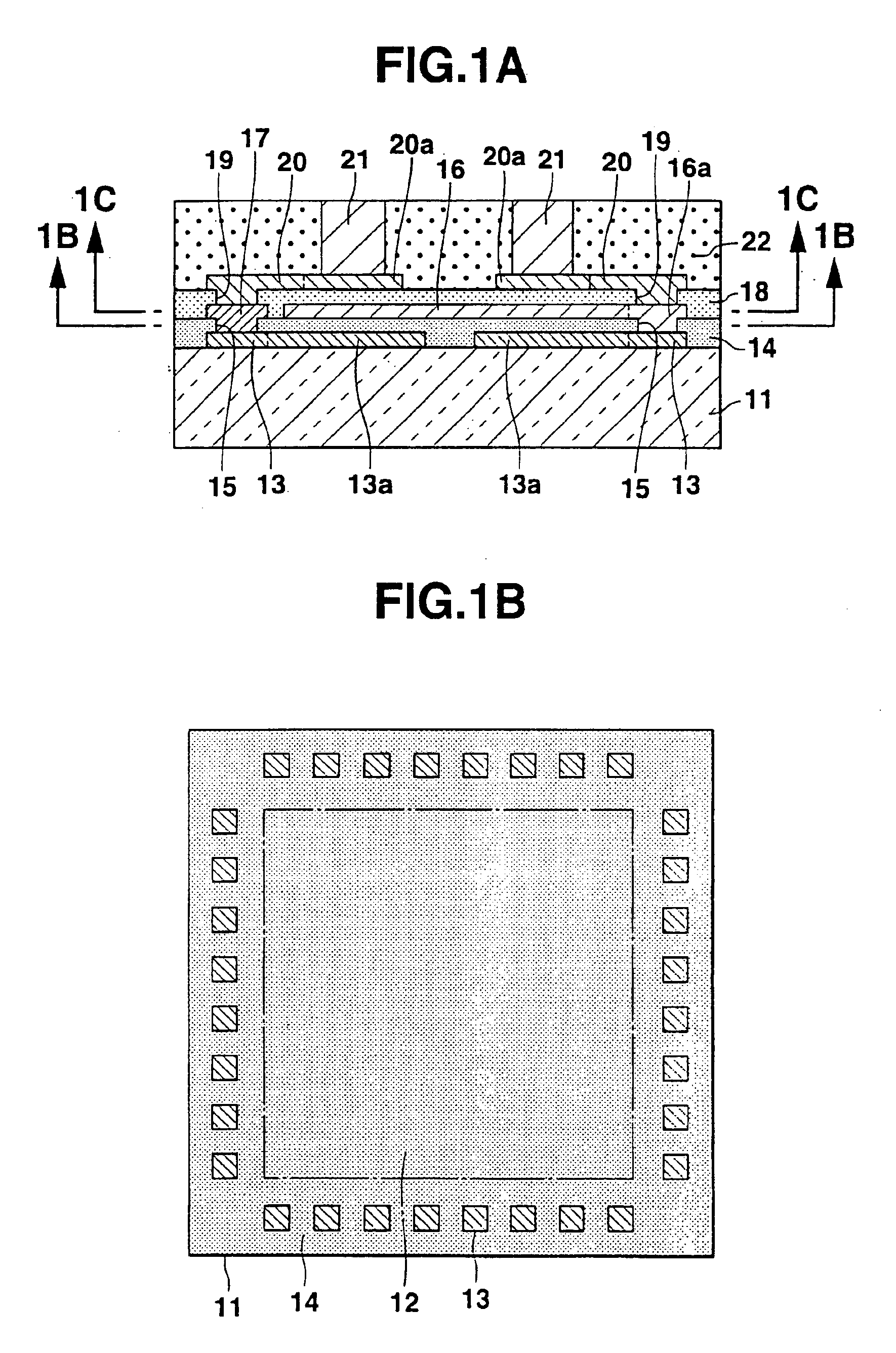
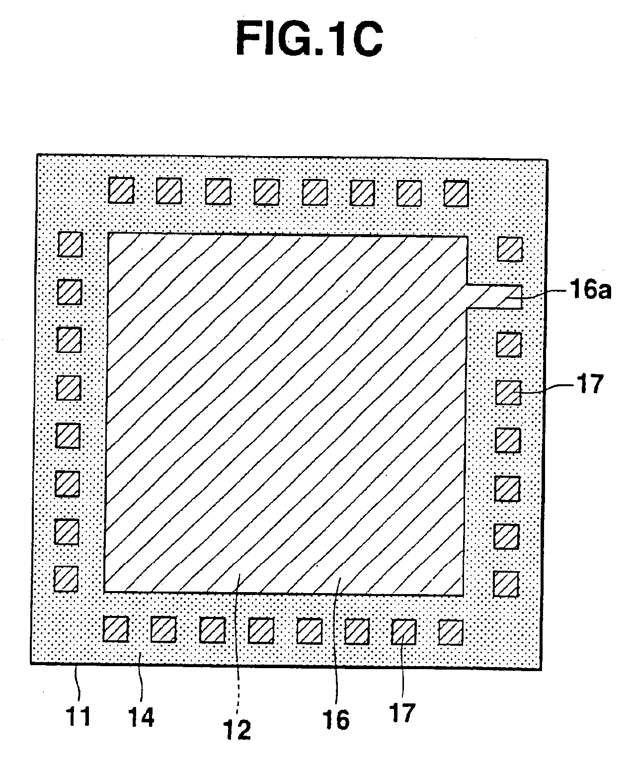
FIG. 1A shows a semiconductor device according to the present invention. FIG. 1B is a cross-sectional view taken along line 1B—1B in FIG. 1A in a state in which connection pad portions 17 are removed. This semiconductor device has a semiconductor substrate 11.

The semiconductor substrate 11 has a rectangular shape, as shown in FIG. 1B. A central region defined by a dot-and-dash line in FIG. 1B serves as a circuit element formation region 12. Where the semiconductor device is an LSI for driving a liquid crystal display panel, an oscillation circuit, a regulator circuit, an LC driver circuit, etc., although not shown, are provided in the circuit element formation region 12. A plurality of connection pads 13 are provided on an upper surface of the semiconductor substrate 11 on the outside of the circuit element formation region 12. Each connection pad 13 is formed of one end portion of a wiring segment 13a extended from the circuit element formation region 12 of semiconductor device 11....

second embodiment

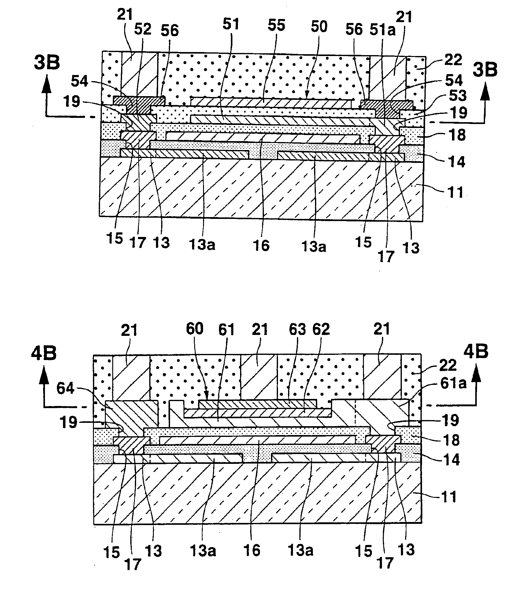
A third embodiment of the invention will now be described with reference to FIG. 2C. FIG. 2C, like FIG. 2B, is a cross-sectional view taken along line 2C—2C in FIG. 2A. A thin-film SAW (Surface Acoustic Wave) filter 41 comprising a pair of interlaced tooth-shaped wiring segments is provided to extend from upper surfaces of predetermined two of the connection pad portions 17 onto the second insulating film 18 provided on the ground potential layer 16 in the circuit element formation region 12. In this case, like the second embodiment, the thin-film SAW filter 41 can be freely arranged without restrictions by virtue of the ground potential layer 16 serving as a barrier layer.

Specifically, in the semiconductor devices according to the second and third embodiments, a thin-film circuit element formed of single-layer wiring is provided in a circuit element formation region with an insulating film interposed, and a ground potential layer serving as a barrier layer for preventing crosstalk ...


PUM


Abstract

In a semiconductor device, re-wiring is provided on a circuit element formation region of a semiconductor substrate. A columnar electrode for connection with a circuit board is provided on the rewiring. A first insulating film is provided over the semiconductor substrate excluding a connection pad, and a ground potential layer connected to a ground potential is provided on an upper surface of the first insulating film. A re-wiring is provided over the ground potential layer with a second insulating film interposed. The ground potential layer serves as a barrier layer for preventing crosstalk between the re-wiring and circuit element formation region. A thin-film circuit element is provided on the second insulating film, and a second ground potential layer is provided as a second barrier layer over the thin-film circuit element with an insulating film interposed. Re-wiring is provided over the second ground potential layer.

Description

BACKGROUND OF THE INVENTIONThe present invention relates to a semiconductor device having columnar electrodes on re-wiring.There is known a semiconductor device called CSP (Chip Size Package). When the semiconductor device is to be mounted on a circuit board, a mounting technique called “face down bonding” is employed. In the case of this type of semiconductor device, columnar electrodes for connection with the circuit board, etc. are provided on a semiconductor substrate or via an intermediate substrate (interposer). FIG. 7A is a cross-sectional view showing an example of this type of conventional semiconductor device, and FIG. 7B is a cross-sectional view taken along line 7B—7B in FIG. 7A in the state in which a protection film 5 and the elements provided thereon are removed. This semiconductor device includes a semiconductor substrate 1 which is, e.g. a silicon substrate.The semiconductor substrate 1 has a rectangular shape, as shown in FIG. 7B. A central region defined by a dot-...

Claims


Application Information

Patent Timeline
IPC IPC(8): H01L23/52H01L23/50H01L23/522H01L23/48H01L31/00H01LH01L21/60H01L21/822H01L21/3205H01L27/00H01L27/04H01L29/40
CPCH01L23/3114H01L23/5223H01L23/5225H01L23/5227H01L23/5228H01L23/525H01L2924/0002H01L2924/1423H01L2924/19041H01L2924/00
Inventor AOKI, YUTAKAMIHARA, ICHIROWAKABAYASHI, TAKESHIWATANABE, KATSUMI
Owner CASIO COMPUTER CO LTD
Why Eureka
Try Eureka