Methods of making microelectronic assemblies including compliant interfaces

a microelectronic assembly and interface technology, applied in the direction of dielectric characteristics, printed circuit aspects, printed element electric connection formation, etc., can solve the problem that the vertical height of the pads cannot be extremely uniform, and achieve the effect of reducing the stress on the connections therebetween and effective encapsulation barrier against moisture and contaminants

Inactive Publication Date: 2005-03-22
TESSERA INC
View PDF41 Cites 55 Cited by
  • Summary
  • Abstract
  • Description
  • Claims
  • Application Information

AI Technical Summary

Benefits of technology

The pads or the pad / injected elastomer combination provide a compliant, planar interface which effectively accommodates for the thermal coefficient of expansion mismatch between the chip and a supporting substrate thereby alleviating much of the stress on the connections therebetween. Further, the combination provides an effective encapsulation barrier against moisture and contaminants.

Problems solved by technology

At this stage of the process, the vertical height of the pads need not be extremely uniform.

Method used


Image

  • Methods of making microelectronic assemblies including compliant interfaces
  • Methods of making microelectronic assemblies including compliant interfaces
  • Methods of making microelectronic assemblies including compliant interfaces

Examples


Embodiment Construction

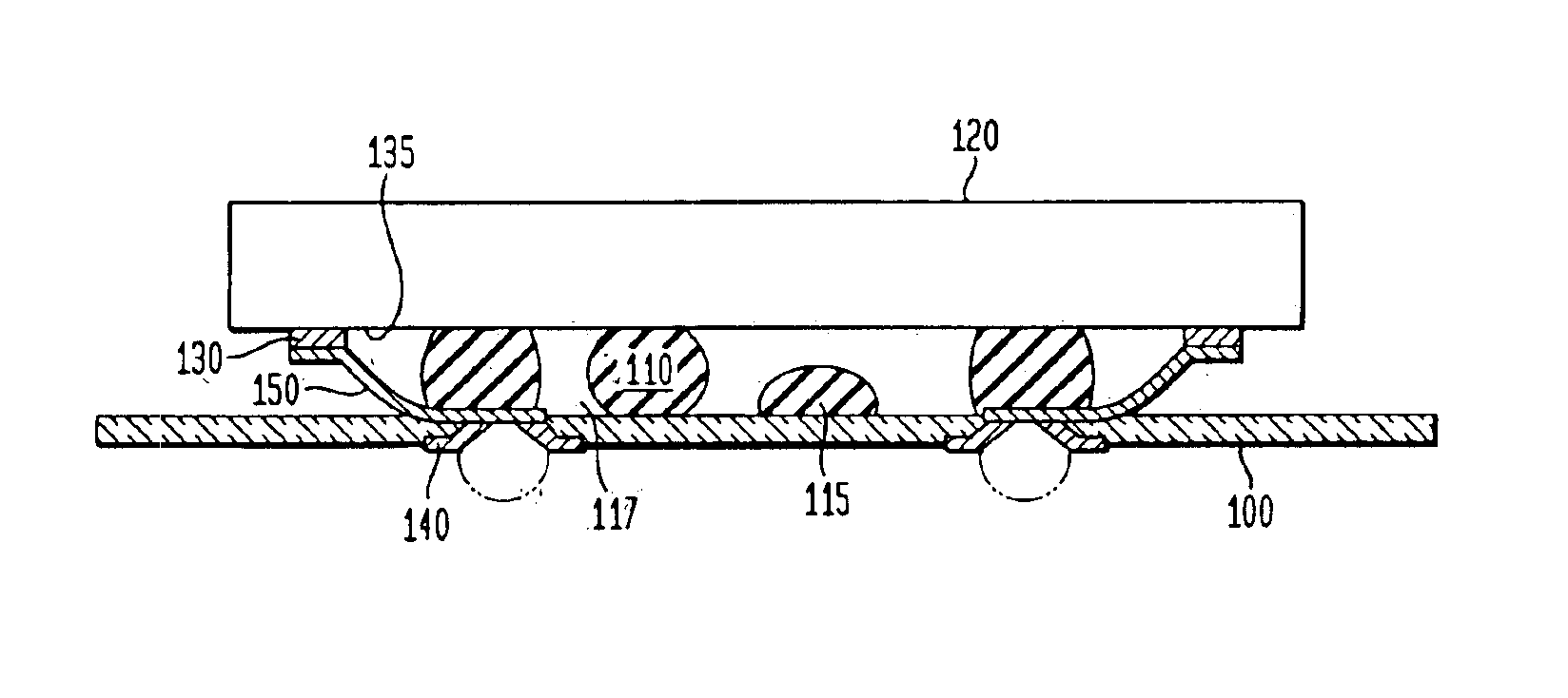
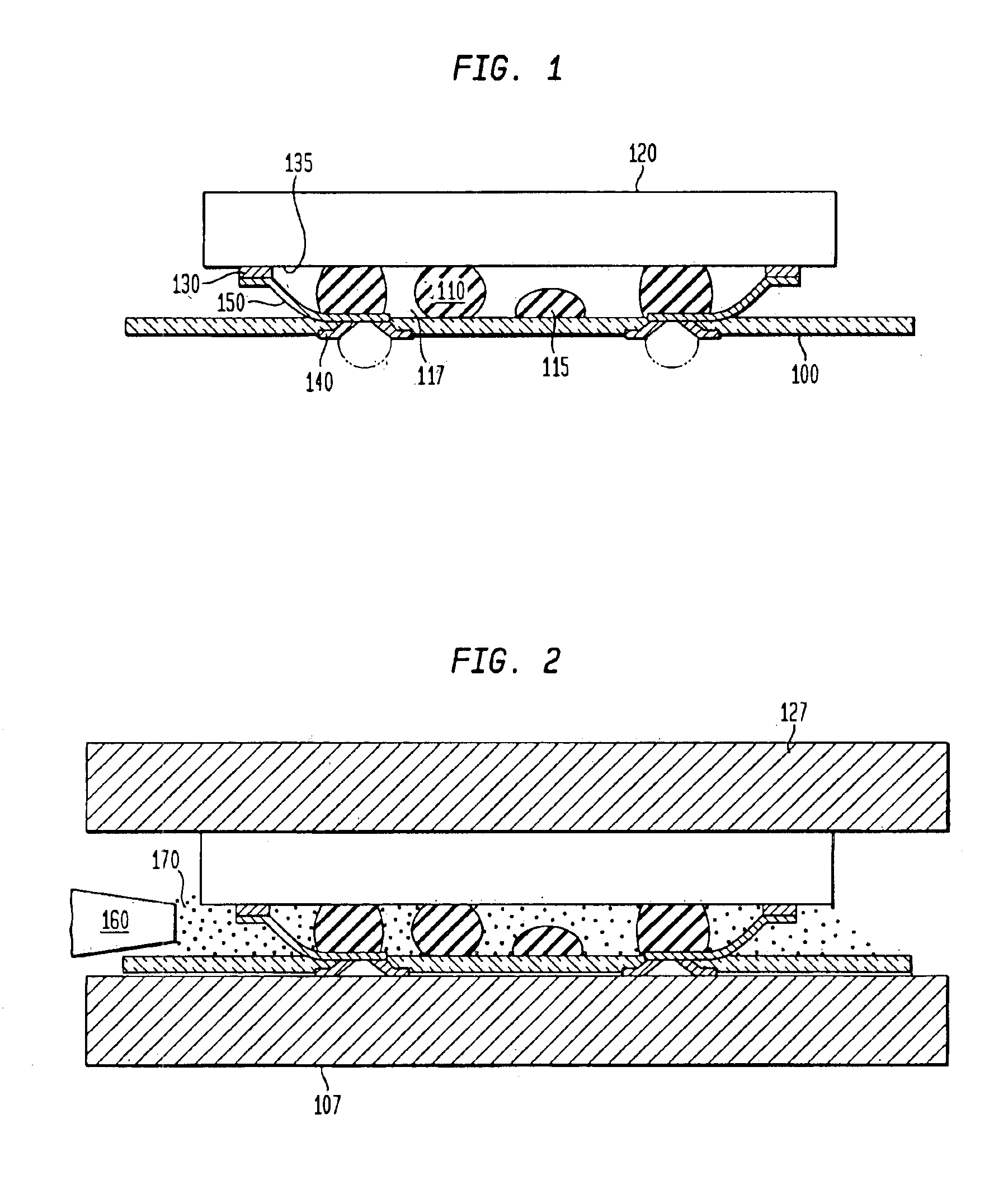
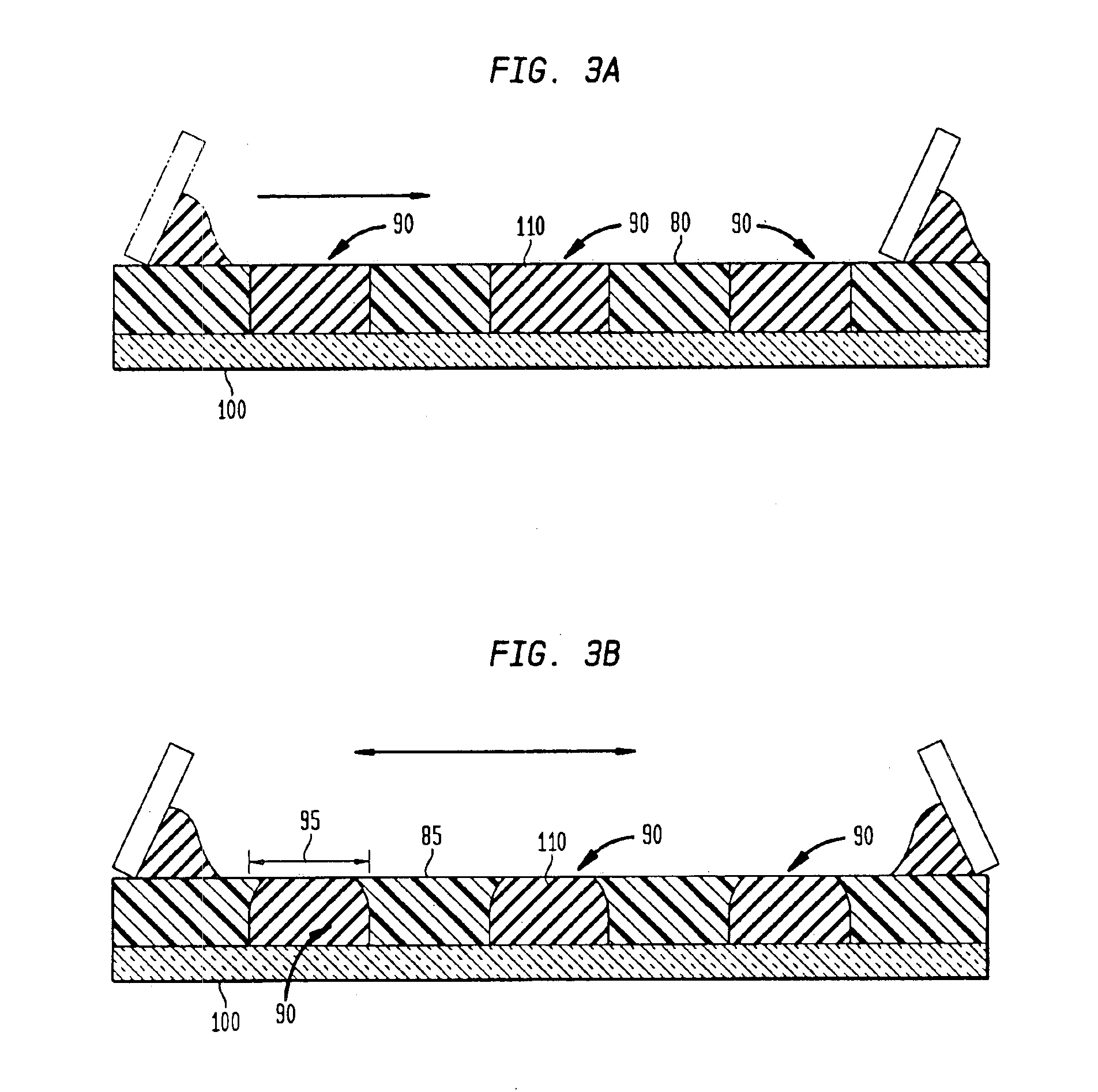
FIGS. 1 and 2 show a side view of a chip size package embodiment, according to the present invention. A support structure 100 is provided having a first and a second surface. The support structure 100 may be substantially rigid, semi-rigid or flexible. However typically, the support structures 100 is comprised of a flexible, but substantially inextensible, dielectric film, preferably formed from a polymeric material, such as KAPTON™“E” available from DuPont Chemical Corp., of an approximate thickness between 25 microns and 75 microns. Further, the dielectric film 100 typically has conductive terminals 140 on its second surface.

A porous layer, such as a layer of a plurality of compliant pads 110, is attached to the first surface of the film 100. The compliant pads 110 are typically made of an curable liquid elastomer material, such as the Dow Corning silicone elastomer 577, known as “Sylgard™”, with about 5-10% of fumed silica in order to obtain a stiff, thixotropic consistency. The ...


PUM


Abstract

An assembly includes a structure, a plurality of terminals and a plurality of compliant pads disposed between said terminals and said structure. The terminals are aligned with at least some of said pads, with the pads providing a standoff between the structure and the terminals. The compliant pads are preferably made of a non-conductive material such as a silicone elastomer.

Description

FIELD OF THE INVENTIONThe present invention relates, generally, to providing a compliant interface for a semiconductor chip, and more particularly relates to a method and apparatus for providing a compliant interface to accommodate for differences in the thermal coefficient of expansion mismatch between a semiconductor chip and a support structure, such as a printed wiring board.BACKGROUND OF THE INVENTIONIn attempting to use the area on printed wiring boards more efficiently, semiconductor chip manufacturers have recently been switching from larger, more cumbersome interconnection conventions, such as pin grid arrays (“PGAs”) and the perimeter leaded quad flat packs (“QFPs”), to smaller conventions, such as ball grid arrays (“BGAs”). Using BGA technology, semiconductor chips are typically interconnected to their supporting substrates using solder connections, such as with “flip-chip” technology. However, when solder alone is used to interconnect the chip contacts to the substrate, ...

Claims


Application Information

Patent Timeline
Patent Type & Authority Patents(United States)
IPC IPC(8): H01L21/56H01L21/60H01L21/02H01L23/498H01L23/48H05K3/40H05K3/36H05K1/11H01L23/31
CPCH01L21/56H01L21/565H01L23/3114H01L23/49811H01L23/49827H01L23/4985H01L24/72H01L24/81H01L24/97H05K3/4084H01L21/563H01L24/29H01L2224/81136H01L23/49816H01L2224/16H01L2224/73203H01L2224/81801H01L2224/83136H01L2224/83192H01L2224/83194H01L2224/97H01L2924/01002H01L2924/01005H01L2924/01013H01L2924/01027H01L2924/01082H01L2924/01322H01L2924/15153H01L2924/15165H01L2924/15311H01L2924/1532H01L2924/16152H01L2924/19041H01L2924/19043H05K1/118H05K3/361H05K2201/0133H05K2201/0394H05K2201/0397H05K2201/09081H05K2203/063H01L2924/014H01L2924/01033H01L2924/01006H01L2224/81H01L2924/3512H01L2924/00H01L2924/351
Inventor KOVAC, ZLATAMITCHELL, CRAIGDISTEFANO, THOMASSMITH, JOHN
Owner TESSERA INC
Why Eureka
Try Eureka