High speed I/O pad and pad/cell interconnection for flip chips

a high-speed semiconductor and flip chip technology, applied in semiconductor devices, semiconductor/solid-state device details, electrical devices, etc., can solve the problems of large parasitic capacitance that has a severe impact on the high-frequency characteristics of the semiconductor chip, cross talk and electromagnetic interference, and large parasitic capacitance, etc., to improve signal transmission, avoid reflection and leakage, and improve the effect of electromagnetic shielding

Inactive Publication Date: 2005-03-22
PMC-SIERRA
View PDF5 Cites 19 Cited by
  • Summary
  • Abstract
  • Description
  • Claims
  • Application Information

AI Technical Summary

Benefits of technology

The invention employs a trace pattern of conductor-backed ground coplanar waveguides (GCPW), which matches impedance at the connection between I/O cells and signal pads to enhance signal transmission, avoid reflection and leakage, a

Problems solved by technology

Such prior art I/O pad arrangements work for low-speed digital and mixed signal integrated circuits, however, suffer from cross talk and electromagnetic interference (EMI) as the semiconductor device's speed and/or frequency increase.
To meet the metal density requirements of semiconductor design rules, dummy metal

Method used


Image

  • High speed I/O pad and pad/cell interconnection for flip chips
  • High speed I/O pad and pad/cell interconnection for flip chips
  • High speed I/O pad and pad/cell interconnection for flip chips

Examples


Embodiment Construction

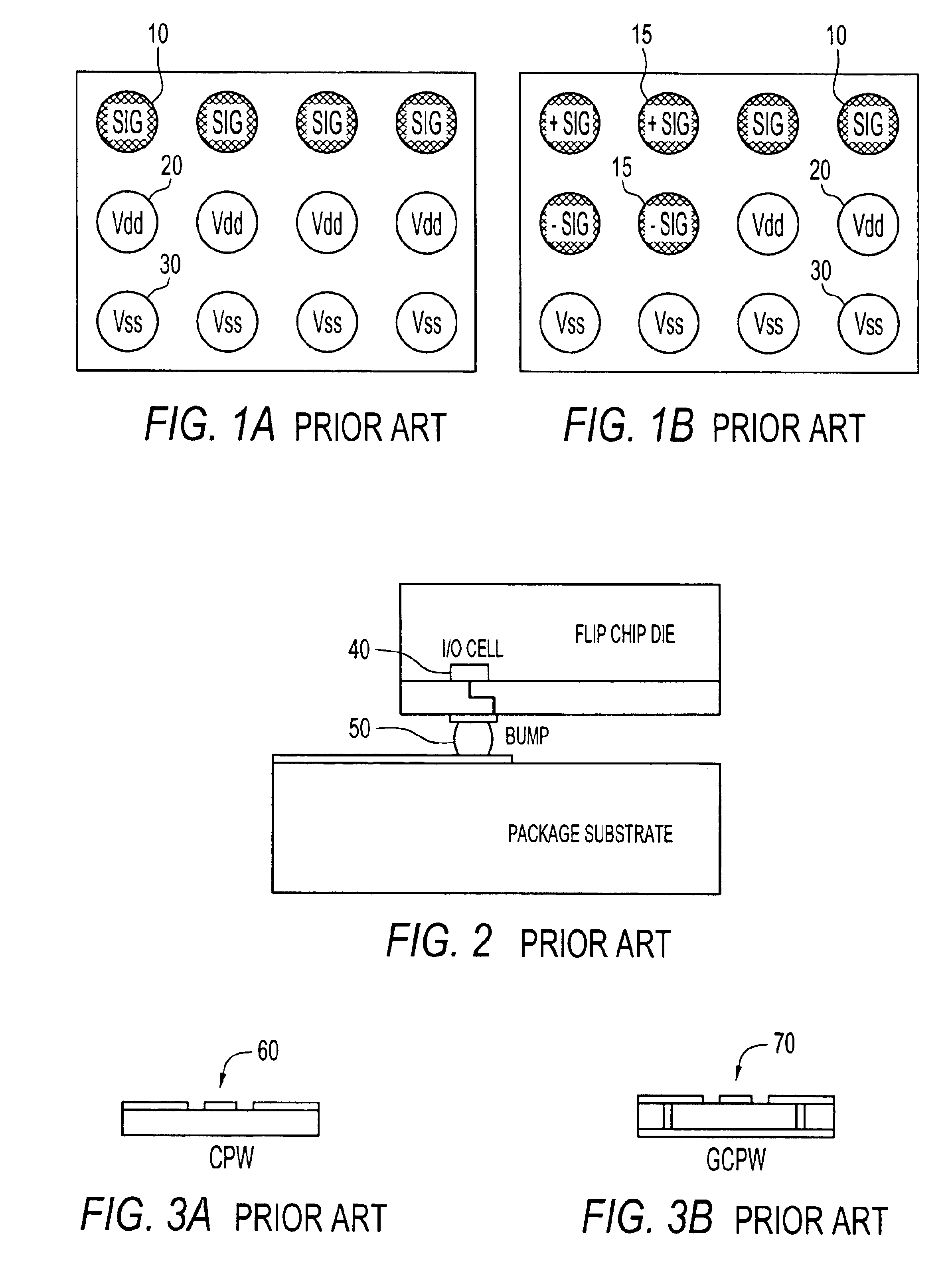
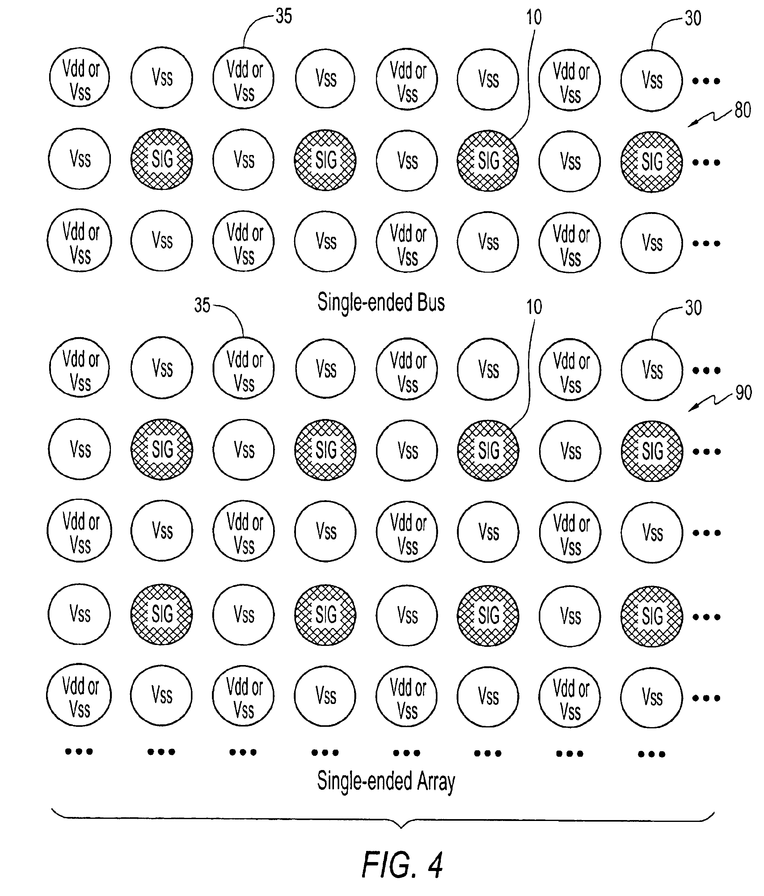
FIG. 4 illustrates a first aspect of the present invention, which comprises a gridded I / O pad concept for single-ended buses 80 and arrays 90 for high-speed or high frequency flip-chip die and packaging applications. The I / O pad configuration comprises signal pads 10, power pads and ground pads 30. Power / ground pads 35 may be either power or ground pads. FIG. 5 illustrates an I / O pad configuration, comprising signal pads 15, power pads and ground pads 30 (power / ground pads 35 may be either power or ground pads) for a differential signal bus 100 and array 110 on a flip chip die. Power / ground pads 35 may be either power or ground pads. Common to each embodiment in FIGS. 4 and 5, is the principle that all of the pads nearest the high-speed signal (SIG) pad 10 or pads (+SIG, −SIG) 15 should be dedicated to ground pads (Vss) 30 while the power / ground pads 35, the ones sitting diagonally with respect to the signal pad 10 or pads 15, should be placed as either power (Vdd) pads or ground (V...


PUM


Abstract

Gridded I/O pads for flip-chip packages in which a coaxial-like solder bump pad configuration is used in which the I/O pads closest to the signal or bump pad are power or ground pads. The ground pads surrounding the signal pad form a coaxial-like pad configuration for impedance matching at the transition from die to package substrate. The ground pads surrounding the signal pad may be connected by a metal trace to form a ground pad ring. The invention employs conductor-backed ground coplanar waveguides (GCPW), which match impedance at connections between I/O cells and signal pads to enhance signal transmission, avoid reflection and leakage, and provide superior electromagnetic shielding. The present invention also supports high quantities of I/Os for a given die size, and supports flexible power and ground placement.

Description

FIELD OF THE INVENTIONThe present invention is related to the field of high-speed or high frequency semiconductor flip-chip die pads and pad / cell interconnection design.DESCRIPTION OF RELATED ARTFlip chip technology provides improved signal integrity and flexible power and ground distribution on a semiconductor die. Flip-chip I / O pad structure consists of signal pads, Vss, (ground) pads and Vdd (power) pads. In the prior art, these pads are generally distributed on the die area such that there is a single array of Vss pads arranged around the periphery of the die. The die is then flipped onto the top of the package and attached with solder bumps. A prior art signal and power / ground pad arrangement, such as that disclosed by Bassett in U.S. Pat. No. 6,242,814, is illustrated in FIG. 1. FIG. 1(a) illustrates the signal 10, Vdd (power) 20 and Vss. (ground) 30 pads placed in a column for a set of single-ended signal I / O cells, and FIG. 1(b) illustrates a mixed pad matrix with differenti...

Claims


Application Information

Patent Timeline
IPC IPC(8): H01L23/52H01L23/50H01L21/60H01L21/02H01L23/552H01L23/48H01L23/528
CPCH01L23/50H01L23/552H01L24/81H01L23/66H01L23/5286H01L2223/6638H01L2224/81801H01L2924/01013H01L2924/14H01L2924/1423H01L2924/15311H01L2924/30105H01L2924/3011H01L2924/3025H01L2924/01005H01L2924/01006H01L2924/01033H01L2924/01076H01L2924/014H01L2224/16225H01L2223/6627H01L2224/05573H01L2224/05568H01L2224/056H01L24/05H01L2924/00014
Inventor TAO, YUMINGLITTLE, VERNON R.
Owner PMC-SIERRA
Why Eureka
Try Eureka