Failure analysis system of semiconductor memory device

Inactive Publication Date: 2005-03-22
RENESAS ELECTRONICS CORP
View PDF13 Cites 21 Cited by
  • Summary
  • Abstract
  • Description
  • Claims
  • Application Information

AI Technical Summary

Benefits of technology

Therefore, an object of the present invention is to provide a semiconductor memory device

Problems solved by technology

For example, if the capacity is increased to 4 times and the number of chips is increased to 2.5 times by use of a large diameter wafer, the number of fail bits will be increased to 10 times. Therefore, in th

Method used


Image

  • Failure analysis system of semiconductor memory device
  • Failure analysis system of semiconductor memory device
  • Failure analysis system of semiconductor memory device

Examples


first embodiment

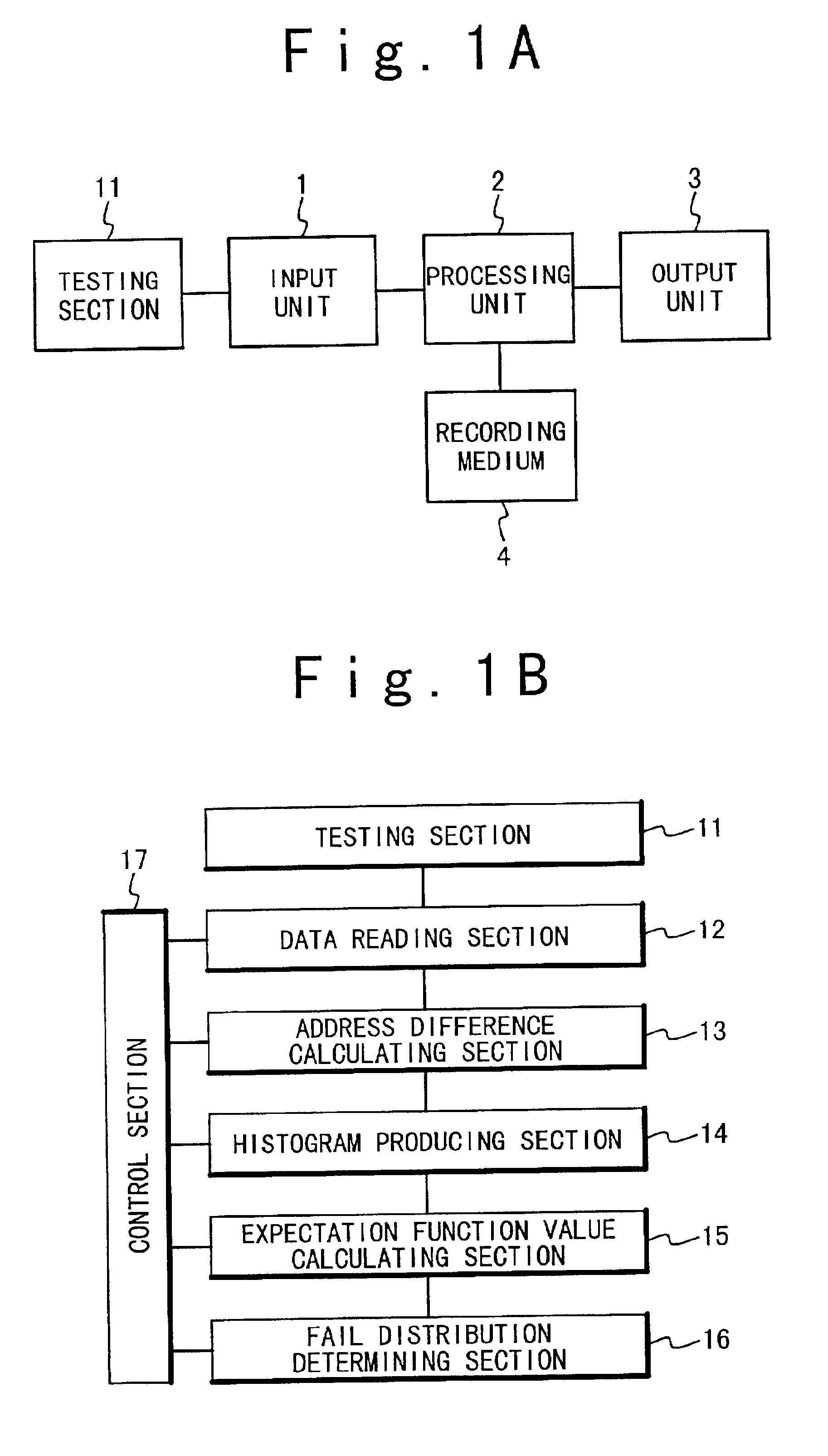
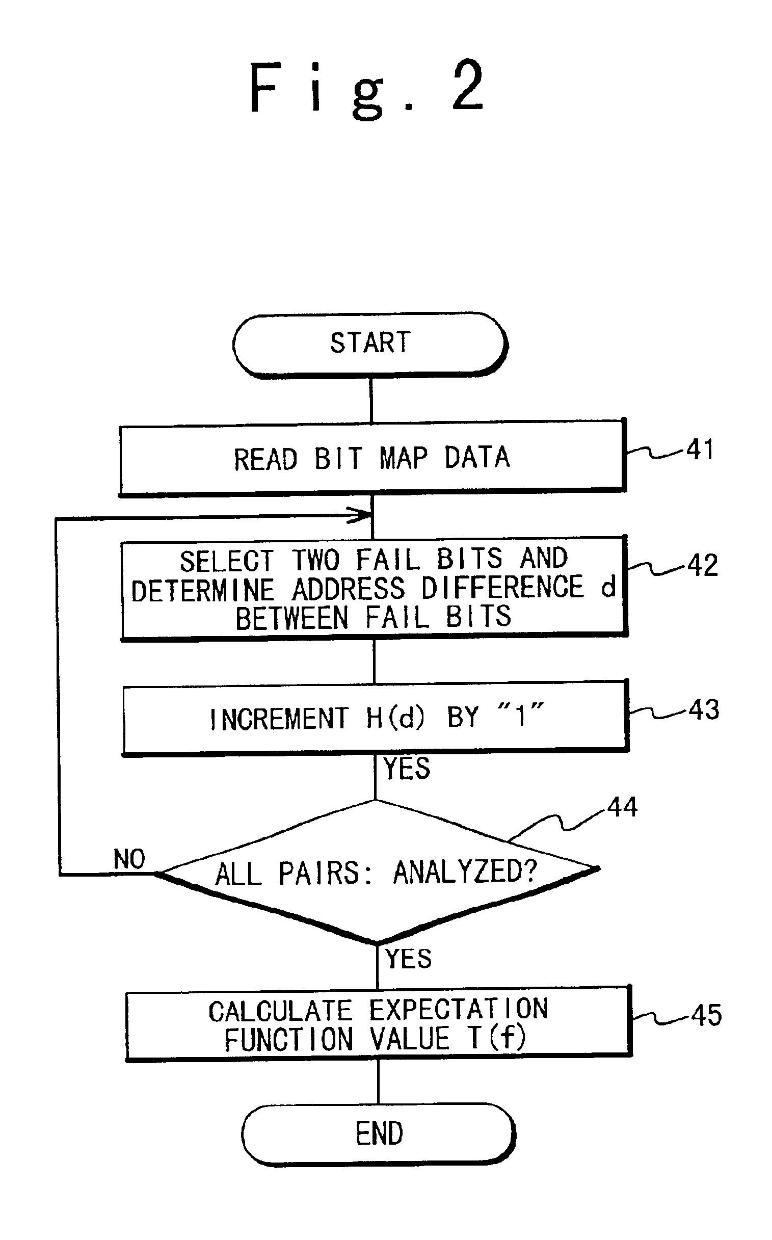
FIG. 1B is a functional block diagram showing the structure of the semiconductor memory device failure analysis system according to the present invention. Also, FIG. 2 is a flow chart showing the processing flow of the failure analysis in the failure analysis system shown in 1.

First, referring to FIG. 1B the semiconductor memory device failure analysis system in the first embodiment is composed of a testing section 11, a data reading section 12, an address difference calculating section 13, a histogram producing section 14, an expectation function value calculating section 15, a fault distribution determining section 16, and a control section 17. The data reading section 12 corresponds to the input unit 1. Also, the address difference calculating section 13, the histogram producing section 14, the expectation function value calculating section 15, the fault distribution determining section 16 and the control section 17 are configured by the processing unit 2. The control section 17 ...

second embodiment

Next, the semiconductor memory device failure analysis system according to the present invention will be described with reference to FIG. 6. Also, the processing flow is shown in the flow chart of FIG. 7.

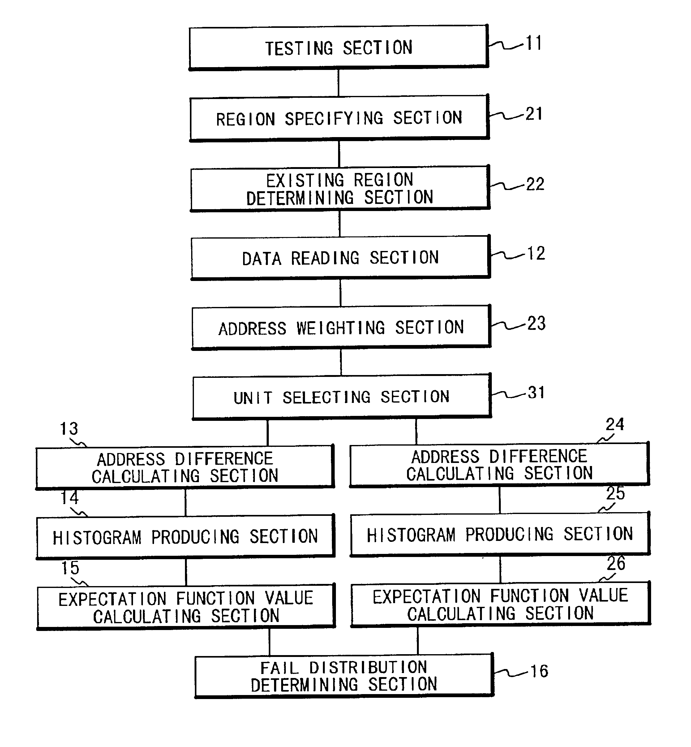
First, referring to FIG. 6, the semiconductor memory device failure analysis system in the second embodiment is composed of the testing section 11, a region specifying section 21, an existing region determining section 22, the data reading section 12, the address weighting section 23, an address difference calculating section 24, a histogram producing section 25, an expectation function value calculating section 26, a fail distribution determining section 16, and a control section 17′. The existing region determining section 22, the address weighting section 23, the address difference calculating section 24, the histogram producing section 25, the expectation function value calculating section 26, the fail distribution determining section 16, and the control section 17′ are configur...


PUM


Abstract

In failure analysis method of a semiconductor memory device, an absolute value of a position difference between two fail bits of a two-dimensional bit map is calculated while a histogram corresponding to the absolute value of the position difference is updated. The bit map indicates a map of fail bits and each fail bit corresponds to a fail memory cell. The above calculation is repeated to all combinations of two of the fail bits in the bit map. Then, an expectation function value is calculated for each of values from the histograms and the number of the fail bits. Finally, whether the fail bits has regularity or irregularity for each value is determined based on the calculated expectation function value for the value.

Description

BACKGROUND OF THE INVENTION1. Field of the InventionThe present invention relates to a failure analysis system of a semiconductor memory device.2. Description of the Related ArtLSI failure analysis apparatuses commercially available from KLA-Tencor and Inspex in United States are conventionally known. These apparatuses are possible to analyze failure in case that about tens of thousands of fails exist on a wafer for semiconductor memory devices.A memory LSI failure analysis apparatus is disclosed in Japanese Laid Open Patent Application (JP-A-Heisei 07-072206) corresponding to Japanese Patent No. 2629523. In this reference, a test result is sent from a memory tester to a personal computer. The know-how of the lay-out technical experts, process technical experts and circuit technical experts is implemented into the personal computer. The personal computer refers to the know-how of the experts to instruct the memory tester to carry out a next test. Thus, a fail cause of the LSI can be...

Claims


Application Information

Patent Timeline
IPC IPC(8): G01R31/28G06F17/50G11C29/00H01L21/66G11C29/56
CPCG11C29/56G11C2029/5604G11C29/00
Inventor TANAKA, MIKIOSUGIMOTO, MASAAKIHAMADA, TAKEHIKO
Owner RENESAS ELECTRONICS CORP
Why Eureka
Try Eureka