
Data transmission circuit for memory subsystem, has switching circuit that selectively connects or disconnects two data bus segments to respectively enable data transmission or I/O circuit connection

a data transmission circuit and memory subsystem technology, applied in computing, instruments, climate sustainability, etc., can solve the problems of reducing the performance of the bus, limiting the maximum speed and bandwidth of the system, and limiting the speed at which data is passed, so as to improve the performance of the high-speed data bus and mitigate the effect of bus reflection

Inactive Publication Date: 2005-03-22
MICRON TECH INC
View PDF12 Cites 145 Cited by
  • Summary
  • Abstract
  • Description
  • Claims
  • Application Information

AI Technical Summary

Benefits of technology

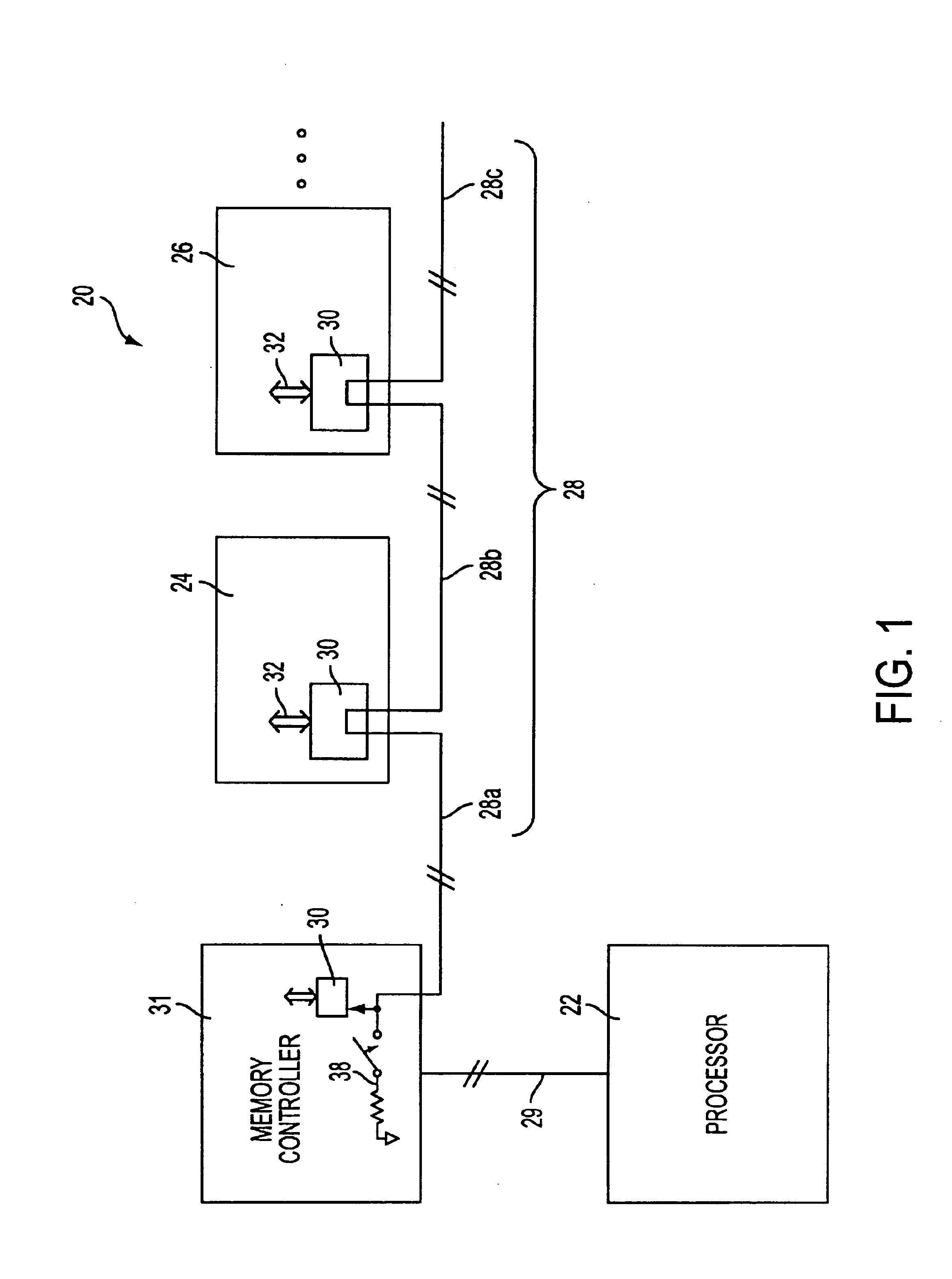
The present invention provides a method and associated apparatus for improving the performance of a high speed data bus, e.g., a memory bus. The invention mitigates bus reflections caused by electrical stubs by connecting contemporaneously-selected system components in a stubless or substantially stubless configuration using switches, for example field effect transistor (FET) or other electronic switches.
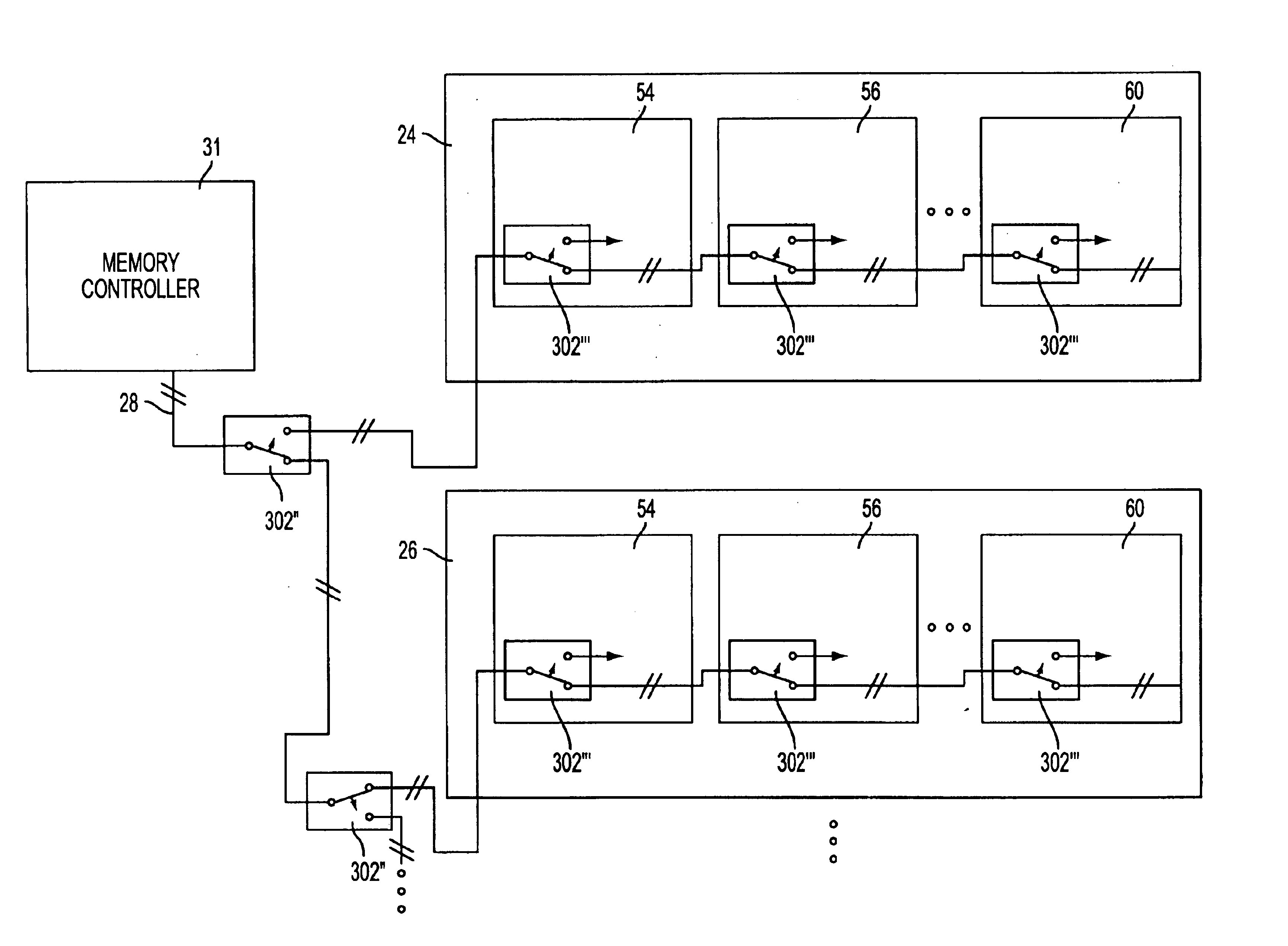
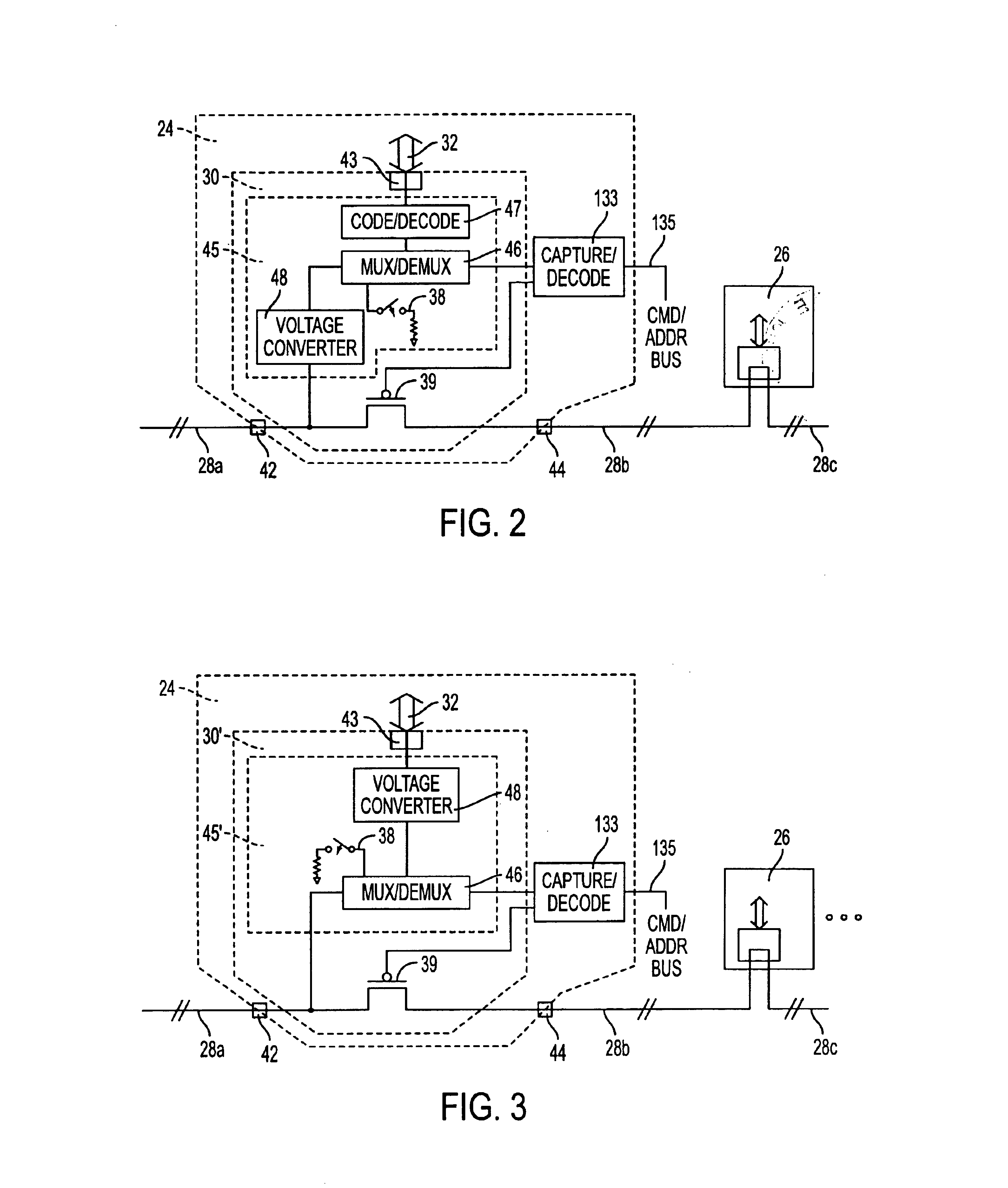
In one aspect, the invention provides a high speed segmented bus in which the individual bus segments are connected by switches. The switches are configured to connect those segments required for communications between currently selected data input / output devices, e.g. memory modules, and disconnect the remaining segments. The resulting bus connects the currently selected data input / output devices in an essentially point-to-point communications configuration for reduced signal reflections and improved signal integrity.

Problems solved by technology

Connection of multiple memory devices to the bus can degrade the performance of the bus since the modules are typically connected in a configuration having electrical stubs which cause signal reflections on the bus.
These reflections degrade signal integrity, thus limiting the maximum speed and bandwidth of the system.
In addition, although high speed communication between memory devices can be done using a transmission line or bus that is properly terminated, the speed at which data is passed can be limited by the capacitance of the memory devices and the resistance of circuit elements used to terminate the bus.
As noted, bus reflections can limit the speed of data transmission as well.

Method used


Image

  • Data transmission circuit for memory subsystem, has switching circuit that selectively connects or disconnects two data bus segments to respectively enable data transmission or I/O circuit connection
  • Data transmission circuit for memory subsystem, has switching circuit that selectively connects or disconnects two data bus segments to respectively enable data transmission or I/O circuit connection
  • Data transmission circuit for memory subsystem, has switching circuit that selectively connects or disconnects two data bus segments to respectively enable data transmission or I/O circuit connection

Examples


Embodiment Construction

The invention provides a bus system including switches which can be used to interconnect data input / output devices and / or bus segments. While the invention is described below with reference to a bus system for a memory system, including memory modules as representative data input / output devices, it should be understood that the bus and switch topology of the invention may be used with any type of data input / output device. Likewise, it should be understood that the memory controller described in the context of a memory system may be a bus controller for use with other data input / output devices besides memory modules.

Referring to FIG. 1, an exemplary processor system 20 including a memory subsystem is illustrated employing a high speed bus system. The processor system 20 includes several data input / output devices, which take the form of memory modules 24, 26, connected to a memory controller 31 with a segmented data bus 28, and a processor 22 connected to the memory controller 31 via ...


PUM


Abstract

A method and associated apparatus is provided for improving the performance of a high speed memory bus using switches. Bus reflections caused by electrical stubs are substantially eliminated by connecting system components in a substantially stubless configuration using a segmented bus wherein bus segments are connected through switches. The switches disconnect unused bus segments during operations so that communicating devices are connected in an substantially point-to-point communication path.

Description

FIELD OF THE INVENTIONThe present invention relates to improving the signal integrity and performance of a high speed bus for data communications.BACKGROUND OF THE INVENTIONMemory device manufacturers are under continuous pressure to increase the performance and reduce the cost of memory devices. Memory systems for computers typically provide many memory devices on a common multidrop bus to allow larger storage and transmission capacities than can be obtained with a single memory device. To improve the maximum throughput of the bus, data communicated to and from the memory devices may be multiplexed for transmission on the bus, thereby reducing the pin count of a memory bus master or controller. For example, a 64-bit wide data word may be transmitted over a 16 bit data bus as four successive 16-bit data word portions.In addition, such systems typically include user upgradable or replaceable components to allow future expansion or repair of the memory subsystems. Typically, these sys...

Claims


Application Information

Patent Timeline
Patent Type & Authority Patents(United States)
IPC IPC(8): G06F13/40G06F13/16G06F13/42
CPCG06F13/1684G06F13/4086G06F13/4265G06F13/4247Y02B60/1235Y02B60/1228Y02D10/00
Inventor GREEFF, ROYOVARD, DAVIDLEE, TERRY R.
Owner MICRON TECH INC
Learn More