
Integrated circuit random access memory capable of automatic internal refresh of memory array

a random access memory and integrated circuit technology, applied in the direction of memory adressing/allocation/relocation, instruments, transistors, etc., can solve the problem of denying the memory bank the opportunity to meet the refresh requirements, and achieve the effect of less space on the integrated circuit and avoiding a delay

Inactive Publication Date: 2005-03-22
INNOMEMORY LLC +1
View PDF12 Cites 30 Cited by
  • Summary
  • Abstract
  • Description
  • Claims
  • Application Information

AI Technical Summary

Benefits of technology

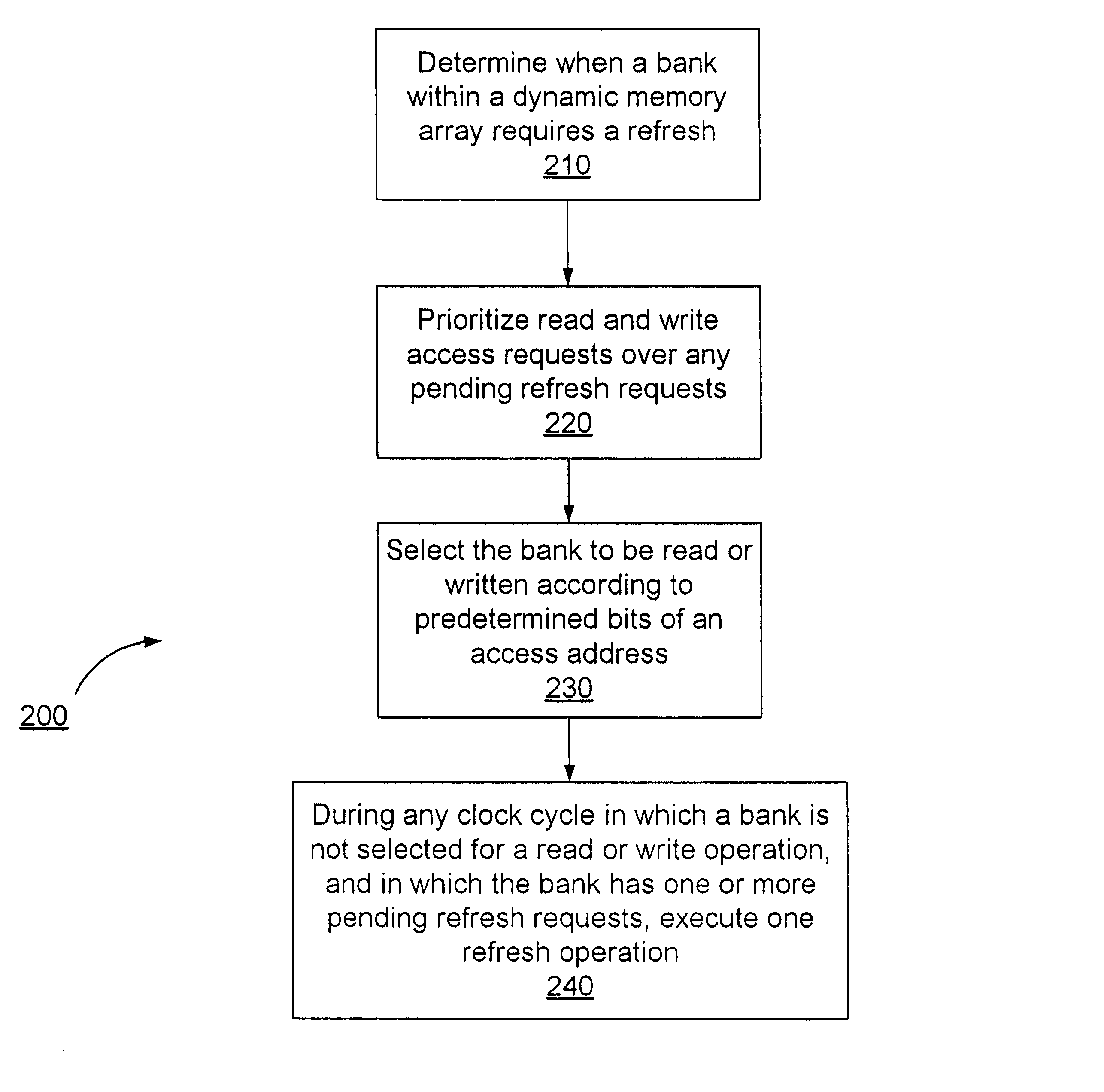
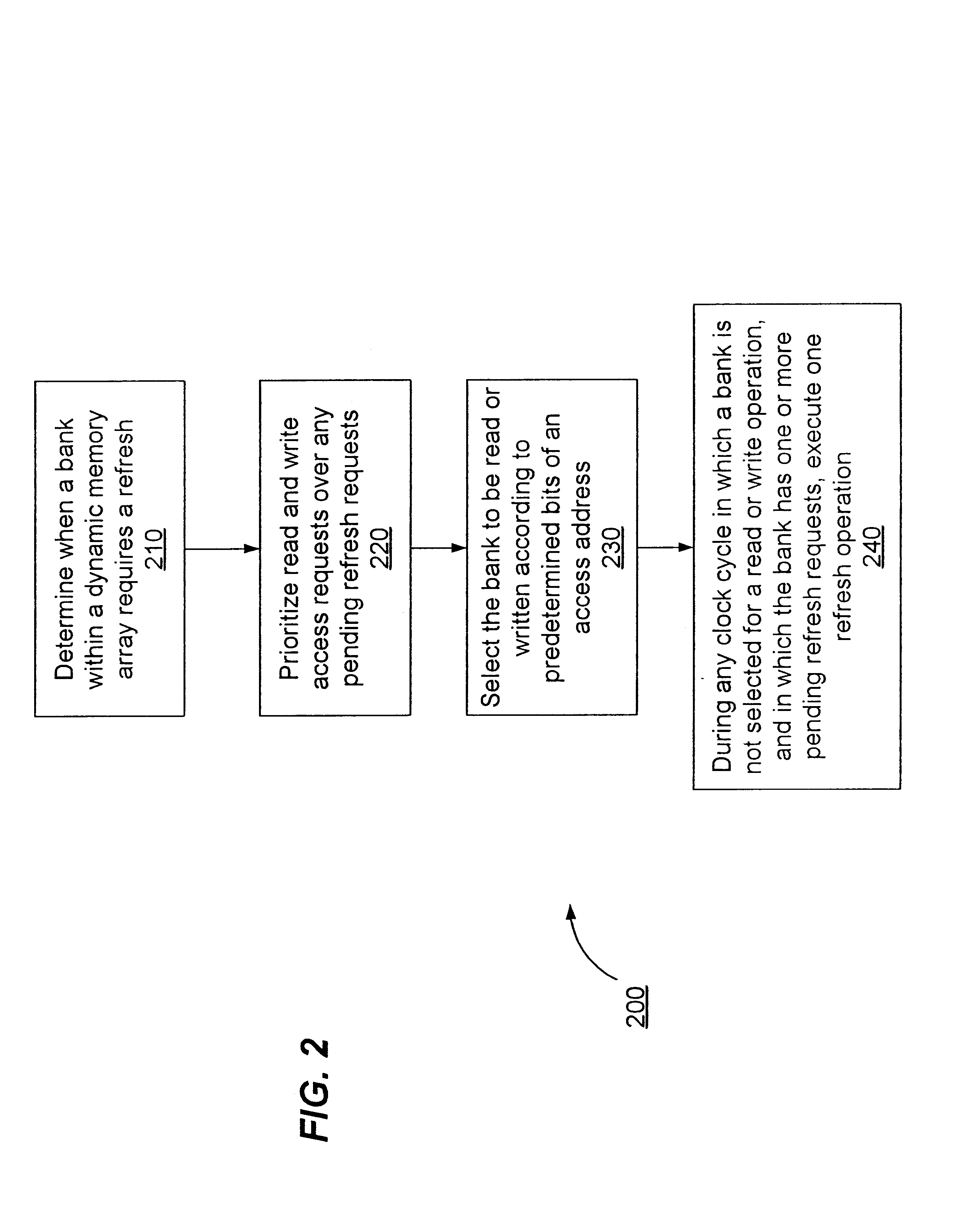
In accordance with the present invention, a random access memory integrated circuit automatically refreshes banks in a dynamic memory array without requiring an on-board cache memory, thereby using less space on the integrated circuit as compared to the space that would be required if a cache memory were to be included. The disclosed random access memory integrated circuit is responsive to an externally supplied clock input and includes a dynamic memory array configured in one or more banks, wherein the array requires periodic refreshing to maintain data. The random access memory integrated circuit further includes one or more refresh control circuits generating refresh requests inside the random access memory integrated circuit. The dynamic memory array is configured to receive read and write access requests that have priority over pending refresh requests. Any pending refresh requests are retired on a clock cycle not requiring an access of the dynamic memory array. Further, the refresh completes in one clock cycle. The read access requests initiate an access to the dynamic memory array without first determining whether data is available from outside the dynamic memory array, (i.e., from an internal cache memory) thereby avoiding a delay associated with such determination.
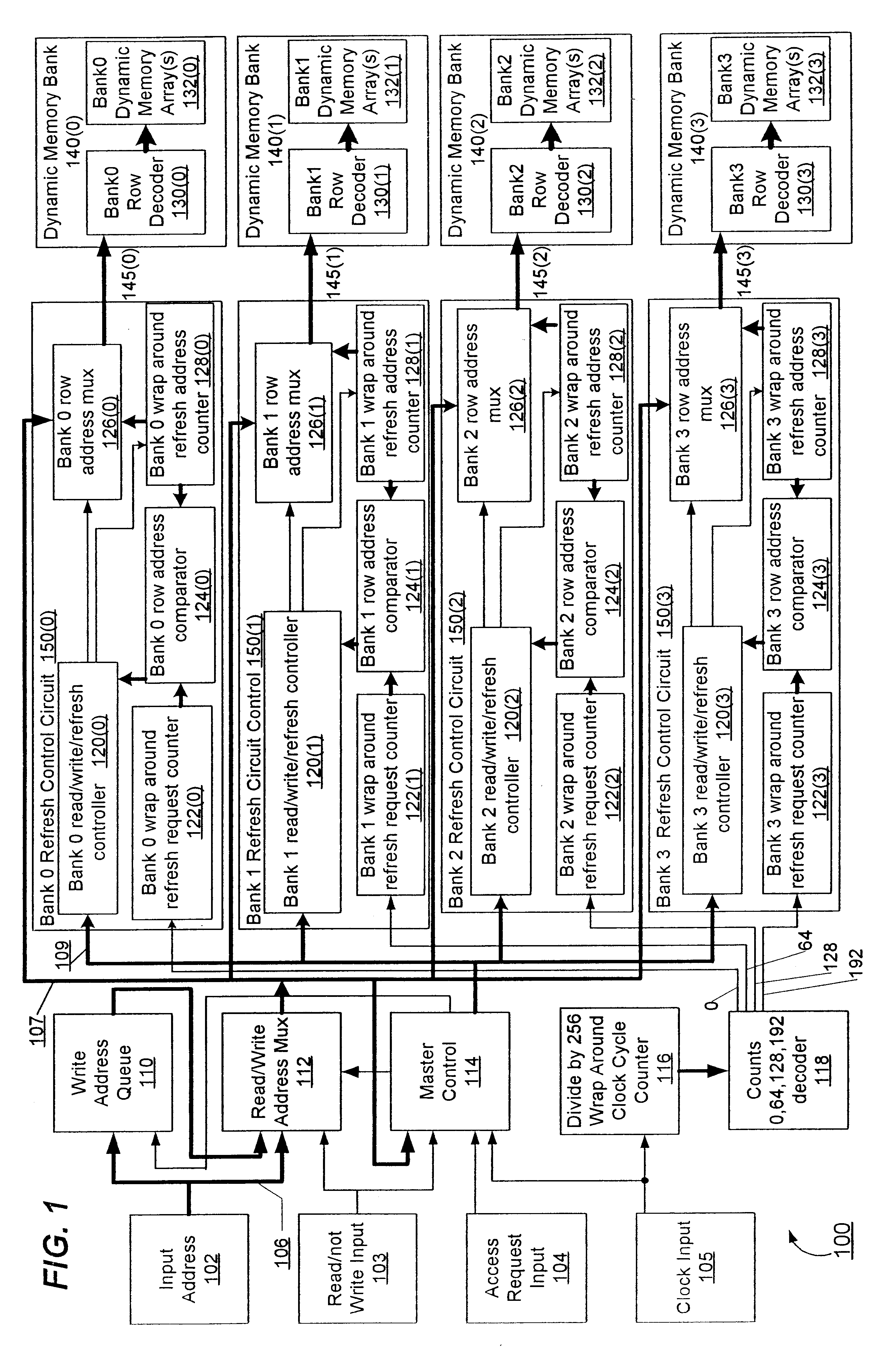
According to a further embodiment containing two or more banks, a separate address bus is coupled to each bank, each of the banks receiving an independent address, wherein at least one bit of the read or write access address is used to select the bank for read or write access. The bit is selected from among low order address bits on the random access memory integrated circuit. In one embodiment, the bit is selected such that the bit changes state frequently. Further, the choice of bits of the address allows the banks to share read and write accessing such that no one bank should require excessive accessing thereby denying that bank the opportunity to meet refresh requirements. Excessive accessing includes accessing the same bank more than 255 read or write cycles of each 256 clock cycles, averaged over many thousands of clock cycles.
Still referring to the refresh control circuit, in another embodiment, each wrap around refresh request counter input within its respective refresh control circuit is coupled to receive a unique output from a decoder; the decoder input is coupled to receive an output from a wrap around clock cycle counter. Every predetermined number of clock cycles, the wrap around clock cycle counter in combination with the decoder cause the decoder to sequentially toggle one of a plurality of outputs. Each decoder output is configured to toggle once at a particular count of the wrap around clock cycle counter, each output to be received by a respective one of the refresh control circuits. The particular counts are the predetermined number of clock cycles apart. The predetermined number of clock cycles is more than a maximum number of queued refresh requests queued in any one refresh control circuit for any bank. The maximum number of queued refresh requests in combination with the larger predetermined number of clock cycles prevent any worst case sequence of external read or write cycles from causing more than two banks to refresh on the same clock cycle.
At least one embodiment of the method includes simultaneously performing access operations and refresh operations on different banks during the same clock cycle. Each refresh control circuit includes a counter configured to increment to reflect a refresh request, the incrementing occurring such that the counter coupled to only one of these banks increments on any given clock cycle. Further, an embodiment limits the number of banks simultaneously performing access operations and refresh operations to not more than three banks to prevent corruption of data by power supply noise.

Problems solved by technology

Further, the choice of bits of the address allows the banks to share read and write accessing such that no one bank should require excessive accessing thereby denying that bank the opportunity to meet refresh requirements.

Method used


Image

  • Integrated circuit random access memory capable of automatic internal refresh of memory array
  • Integrated circuit random access memory capable of automatic internal refresh of memory array
  • Integrated circuit random access memory capable of automatic internal refresh of memory array

Examples


Embodiment Construction

Overview

An embodiment of the present invention is directed to a memory device including internal refresh control circuitry for automatically performing refresh of the memory array without user intervention and almost always without access interruption. A separate refresh control circuit is provided for each memory bank, each control being configured to execute a refresh operation, for its respective memory bank, during the first available cycle following a refresh request which request occurs once every, for example, 256 external clock cycles.

Unlike most earlier devices, an embodiment is directed to “hidden” refresh cycles that can fully complete in just one clock cycle, allowing a read or write access cycle to begin in the same memory bank on the very next clock cycle, if required, in accordance with a next command and address received. Thus, even if the memory bank is free for only one cycle, a hidden refresh operation can be fully performed and the memory bank ready on the very n...


PUM


Abstract

A dynamic random access memory integrated circuit and method includes internal refresh control and an array configured to receive read and write access requests having priority over pending refresh requests, wherein refresh requests are queueable and retired on clock cycles not requiring an access of the array and complete in one clock cycle. No onboard cache memory is required. A method includes: determining within the circuit when one of the banks of the array requires a refresh, prioritizing read and write access requests over pending refresh requests, read access requests initiating an access to the array without determining whether data is available from outside the array, and retiring within a clock cycle one pending refresh request to a bank when that bank has pending refresh requests and does not also require an access of the array on that clock cycle.

Description

BACKGROUND OF THE INVENTION1. Field of the InventionThe present invention relates to semiconductor memories, and particularly to architecture and organization of a dynamic random-access memory array having automatic internal refreshing of the memory array.2. Description of Related ArtSemiconductor random-access memory devices or sub-systems using arrays of dynamic memory cells (e.g., 1-transistor / 1-capacitor (1T / 1C) cells) have consistently provided greater density and lower cost per bit than those using static memory cells (e.g., 6-transistor (6T) cells, or 4-transistor / 2-resistor (4T / 2R) cells). However, such dynamic random-access memory arrays have historically had lower operational frequencies and longer read access times when compared to static random-access memory arrays. Consequently, system designers have typically chosen dynamic memory arrays (e.g., commercially available dynamic random access memories, or DRAMs) when high density and low cost are required, such as for CPU ...

Claims


Application Information

Patent Timeline
IPC IPC(8): G11C11/4091G11C7/12G11C7/00G11C7/18G11C7/06G11C7/22G11C8/00G11C8/08G11C11/4076G11C11/409G11C11/407H01L27/108H01L21/70H01L21/8242
CPCG11C7/065G11C7/12G11C7/18G11C7/22G11C8/08G11C11/406G11C11/4091H01L27/10897G11C11/4076G11C2207/104G11C2207/229H01L27/10891H10B12/50H10B12/488G11C11/40618G11C11/4087
Inventor PROEBSTING, ROBERT J.
Owner INNOMEMORY LLC
Learn More