

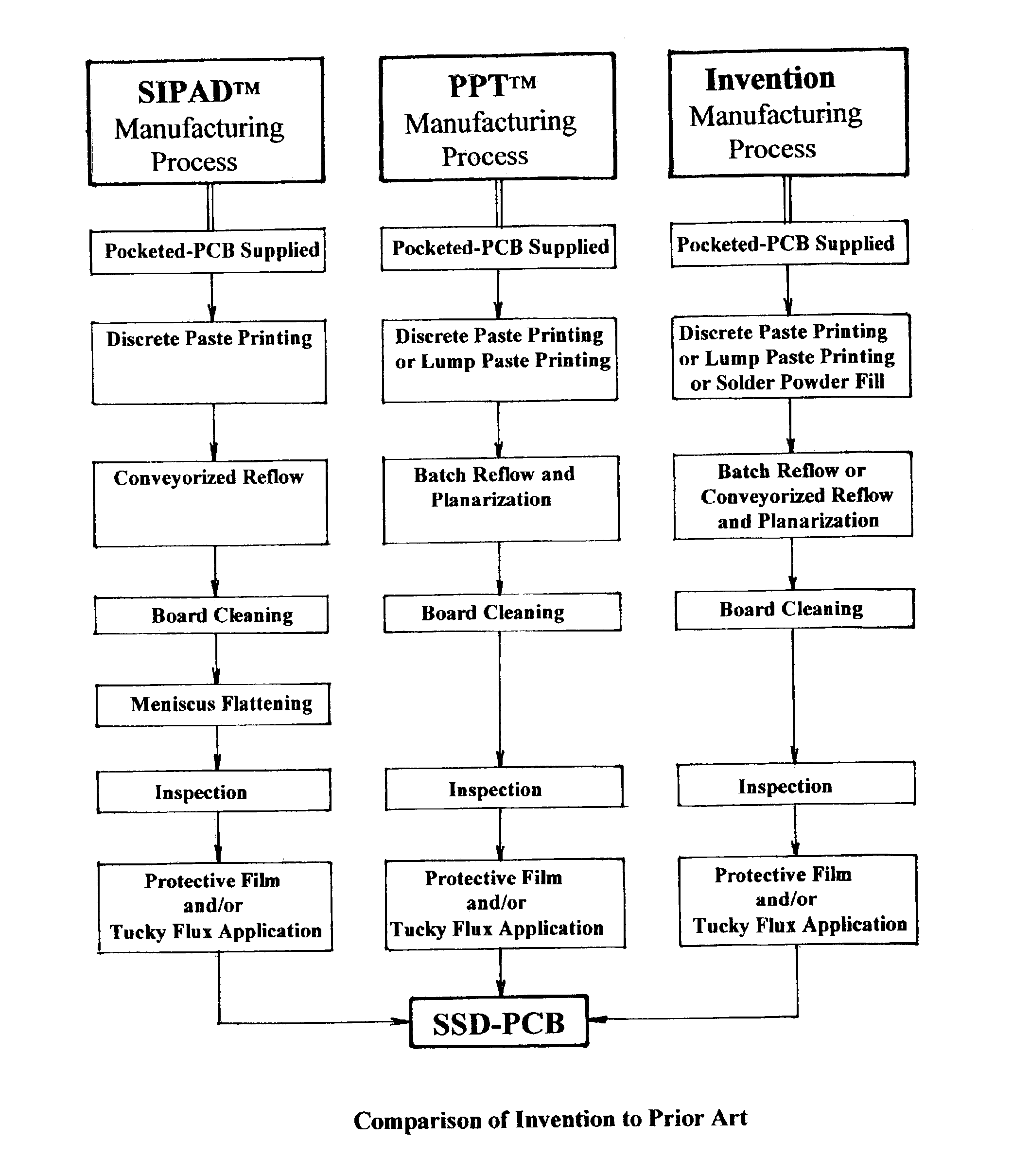
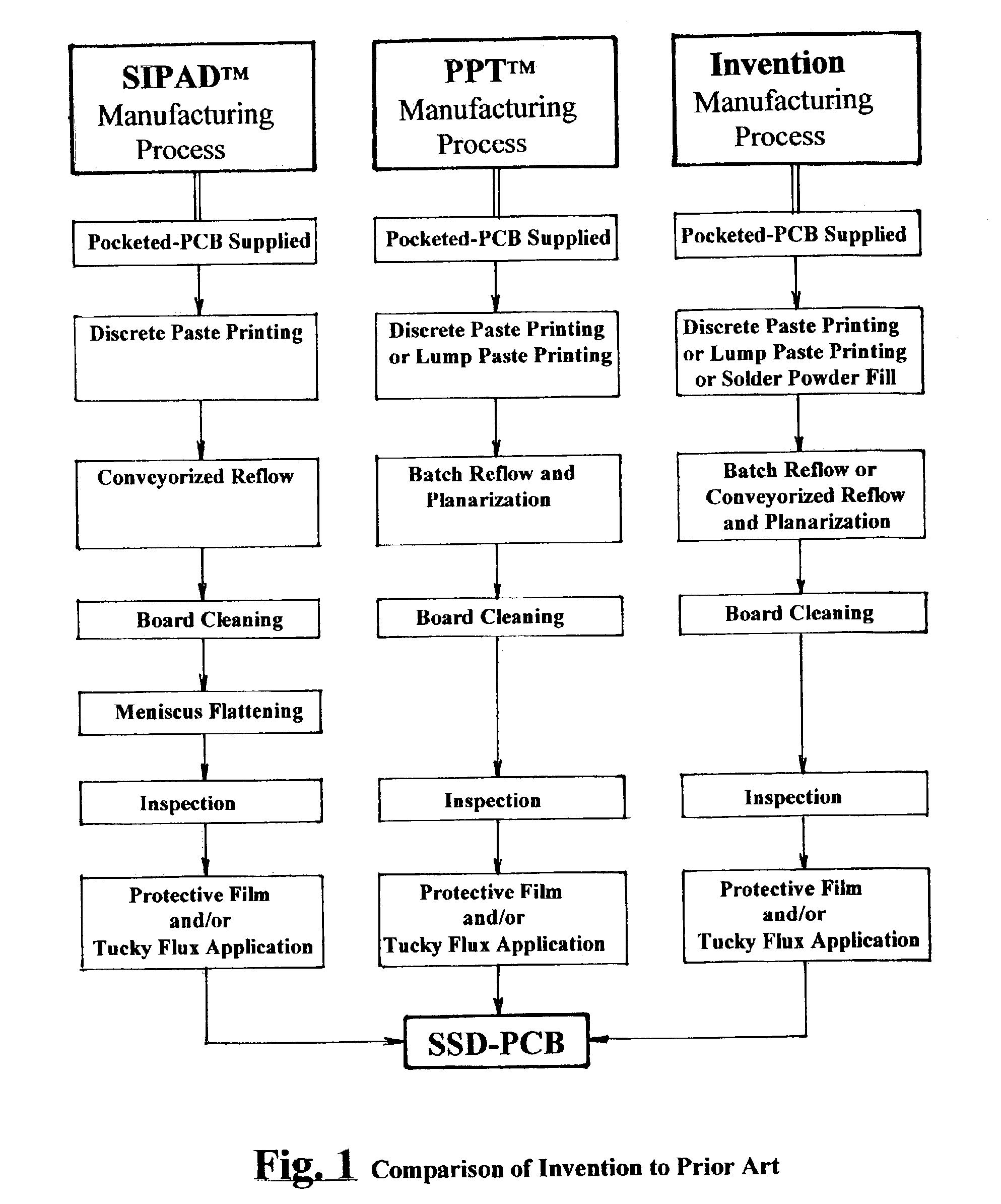
Manufacture of solid-solder-deposit PCB utilizing electrically heated wire mesh
a technology of electrically heated wire mesh and manufacturing process, which is applied in the direction of manufacturing tools, welding/cutting media/materials, and manufacturing tools
- Summary
- Abstract
- Description
- Claims
- Application Information
AI Technical Summary
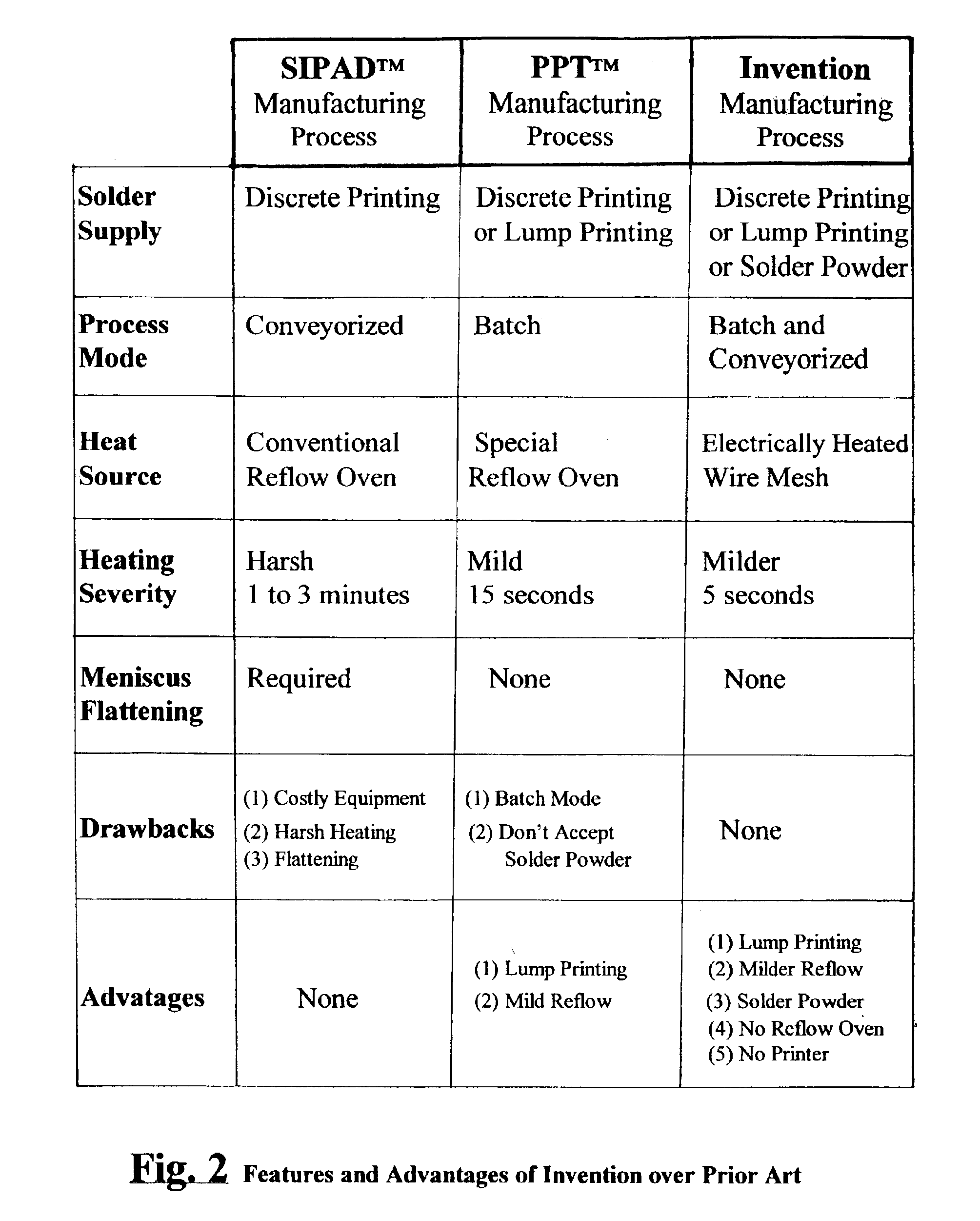
Benefits of technology
Problems solved by technology
Method used
Image

Examples
second embodiment
my invention intended for batch manufacture of SSD-PCB utilizing dry solder powder instead of solder paste is shown in FIG. 10 illustrated in accordance with the objectives of my invention by comprising a pocketed-PCB 20 (itself comprising a multiplicity of upward facing pockets 30 each filled with a solder powder pile 38), a mesh assembly 48 (itself comprising a tightened wire mesh 50, a pair of mesh end anchors 52—52 and a pair of link rods 54—54), a workholder 56 where pocketed-PCB 20 and mesh assembly 48 are both resting and clamped down by means not shown in the figure such as that said mesh 50 is pressing down mesh 50 against pocketed-PCB 20 upper face, means not shown to supply a predetermined electric current to mesh 50 via both mesh end anchors 52—52, means not shown to induce vibration onto said workholder 56, an enclosure chamber 58 that permits to contain vapors and / or gases generated during operation that may cause occupational health hazards and / or safety risks, means ...
third embodiment
my invention intended for conveyorized manufacture of SSD-PCB is shown in FIG. 11 illustrated in accordance with the objectives of my invention by comprising a twin-conveyor system 66 itself comprising a conveyor belt 68, a driver drum 70, a driven drum 72, a set of idle rollers 74, a conveyor wire mesh 76, a driver spool 78, a driven spool 80, means not shown for causing belt 68 and wire mesh 76 to move at the same tangential speed, a pair of mesh electrodes 82—82 capable of being lowered and then retracted, means not shown to supply an electric current to electrodes 82—82, a vibration inducer 84, a fumes hood chamber 86 that permits to contain vapors and / or gases generated during operation that may cause occupational health hazards and / or safety risks, means not shown to remove in an environmentally safe manner said vapor and / or gases, a controllable inlet / outlet means 88 for supplying a process gas (such as Nitrogen or Argon) to said enclosure chamber 86, mesh scraping means 90, ...
fourth embodiment
my invention intended for conveyorized manufacture of SSD-PCB utilizing dry solder powder instead of solder paste is shown in FIG. 22 illustrated in accordance with the objectives of my invention by comprising the same elements recited above for the case of FIG. 11 and in addition comprising a flux stencil 108, a flux supply volume 110, a doctor blade 112 and a flux printing station 114.
In operation a pocketed-PCB 20 (itself comprising a multiplicity of upward facing pockets 30 each filled with a dry solder powder pile 38) is captured at board capture station 96 by conveyor belt 68 and conveyor wire mesh 76 (entrapped in a sandwiched fashion) at board capture station 96 since both said conveyors form a narrow moving passage 106. Once pocketed-PCB 20 arrives at flux printing station 114 belt 68 and mesh 76 both stop.
Immediately, flux stencil 108 is placed on top of mesh 76 in proper alignment with pocketed-PCB 20 utilizing alignment (or registration) means not shown in the figure. Th...
PUM
| Property | Measurement | Unit |
|---|---|---|
| temperature | aaaaa | aaaaa |
| temperature | aaaaa | aaaaa |
| volumes | aaaaa | aaaaa |
Abstract
Description
Claims
Application Information