Light emitting device

a technology of light emitting devices and light emitting elements, which is applied in the direction of static indicating devices, solid-state devices, instruments, etc., can solve the problems of inability to obtain desirable light emission intensity, variation in the amount of current supplied to the light emitting element, and the effect of suppressing the influence of a variation in the characteristics of the driver transistor

Inactive Publication Date: 2005-03-29
SEMICON ENERGY LAB CO LTD
View PDF7 Cites 45 Cited by
  • Summary
  • Abstract
  • Description
  • Claims
  • Application Information

AI Technical Summary

Benefits of technology

The present invention has been made in view of the above problems, and has an object thereof to provide a light emitting device in which the influence of deterioration of a light emitting element resulting from a change over time is suppressed. In addition, another object of the present invention is to provide a light emitting device in which the influence of a variation in characteristics of a driver transistor is suppressed. Further, another of the present invention is to provide a light emitting device capable of simplifying a complicated manufacturing process resulting from manufacturing of transistors having different conductivity types on the same insulating surface.

Problems solved by technology

More specifically, when a voltage-current characteristic of the light emitting element is deteriorated due to a change over time, the amount of current flowing between both electrodes of the light emitting element becomes smaller, so that a desirable light emission intensity cannot be obtained.
However, when characteristics such as mobility and a threshold value of the driver transistor are varied, there is caused a variation in the amount of current supplied to the light emitting element.
Thus, unevenness of the entire display screen is caused.
Therefore, a complicated process in which transistors having different conductivity types are manufactured on an insulating surface or a semiconductor substrate causes a reduction in yield and a rise in cost.

Method used


Image

  • Light emitting device
  • Light emitting device
  • Light emitting device

Examples


embodiment 1

[Embodiment 1]

In this embodiment, a configuration and an operation of a pixel provided in a light emitting device of the present invention will be described with reference to FIG. 4B.

First, a detailed configuration of a pixel 101 in this embodiment will be described with reference to FIG. 4B. In the pixel 101, reference numerals 111 to 114 and 126 denote switches, 120 denotes a light emitting element, 121 denotes a signal line, 122 denotes a scanning line, 123 denotes a power source line, and 119 and 127 denote capacitor elements.

The switches 111 and 126 are connected in series and the switches 112 to 114 are connected in series with one another. In addition, the capacitor element 119 and the light emitting element 120 are connected in parallel. Note that elements each having a switching function are desirably used for the switches 111 to 114 and 126, preferably, transistors are used therefor. When transistors are used for the switches 111 to 114 and 126, it is necessary to provide ...

embodiment 2

[Embodiment 2]

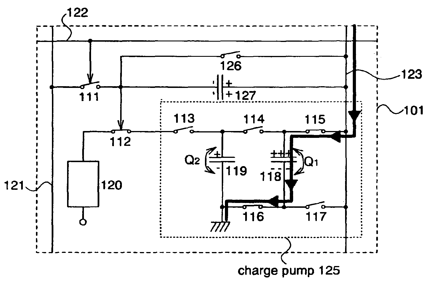
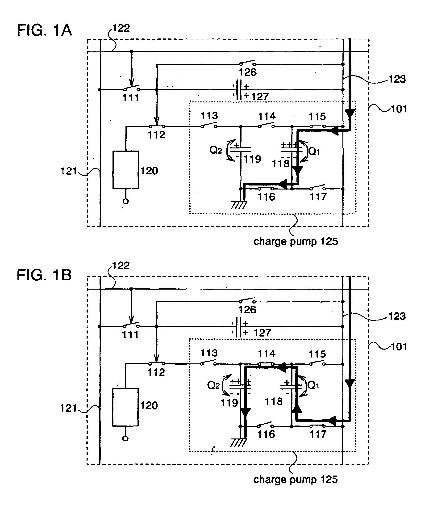
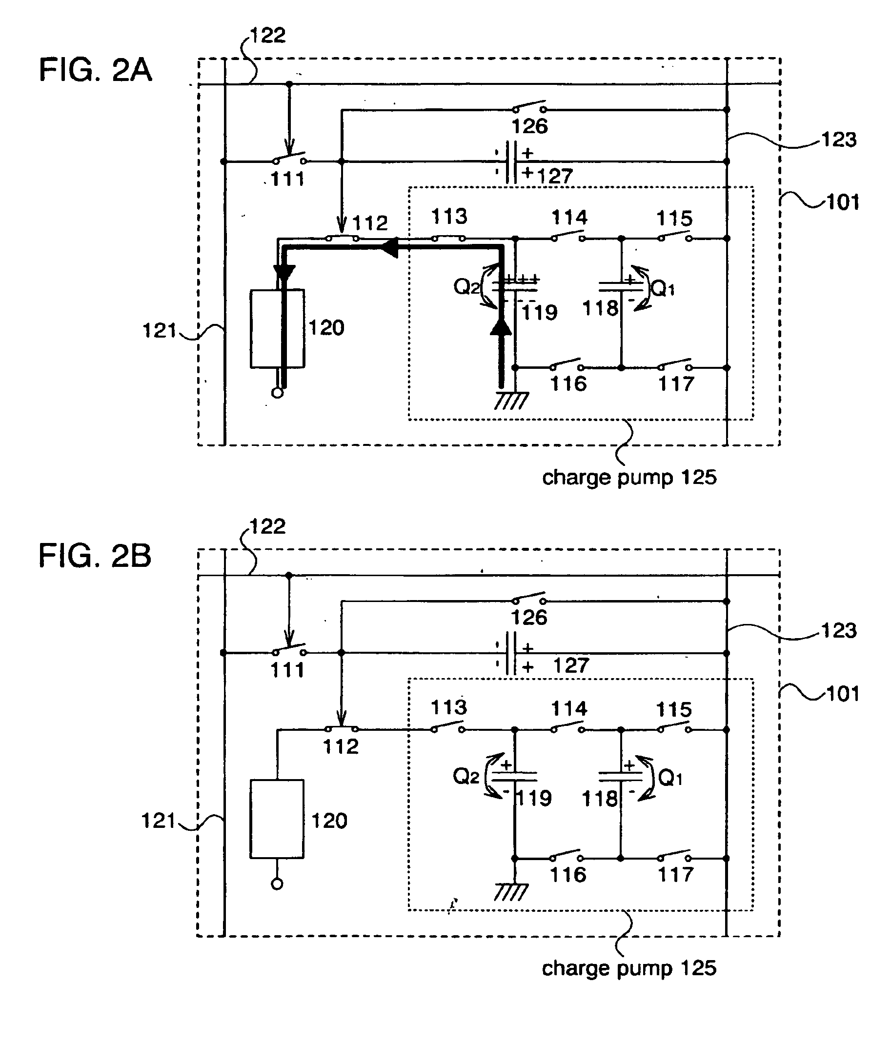
In this embodiment, a detailed configuration and an operation of a pixel provided in a light emitting device of the present invention will be described with reference to FIGS. 1A, 1B, 2A, and 2B.

First, a detailed configuration of a pixel 101 in this embodiment will be described with reference to FIG. 1A. In the pixel 101, reference numerals 111, 112, and 126 denote switches, 120 denotes a light emitting element, 121 denotes a signal line, 122 denotes a scanning line, 123 denotes a power source line, 125 denotes a charge pump (booster pump), and 127 denotes a capacitor element. The charge pump 125 includes switches 113 to 117 and capacitor elements 118 and 119.

The switches 111 and 126 are connected in series, the switches 112 to 115 are connected in series, and the switches 116 and 117 are connected in series with each one another. In addition, the capacitor elements 118 and 119 are connected in parallel. Note that elements each having a switching function are desirably...

embodiment 3

[Embodiment 3]

In this embodiment, a configuration of a pixel 101 which is different from that in the above-mentioned embodiment will be described with reference to FIGS. 3A, 3B, and 4A.

The pixel 101 shown in FIG. 3A has a configuration in which the switches 116 and 117 are excluded in the pixel 101 shown in FIGS. 1A, 1B, 2A, and 2B. In addition, a clock signal is directly inputted to one electrode of the capacitor element 118. Because the detailed description for the configuration and operation of the pixel 101 shown in FIG. 3A is analogous to the above-mentioned embodiment, the description is omitted here.

According to the configuration of the pixel 101 shown in FIG. 3B, a capacitor element 141 and switches 142 to 144 are added to the pixel 101 shown in FIGS. 1A, 1B, 2A, and 2B, thereby increasing the number of stages in a charge pump 125 by one stage to three stages. In the pixel 101, a charge A flowing into the light emitting element 120 can be indicated by the following equation ...


PUM


Abstract

In order to suppress the influence of deterioration of a light emitting element resulting from a change over time, the present invention provides a light emitting device in which an electrical circuit for flowing a constant charge between both electrodes of the light emitting element is provided in each pixel. In addition, the present invention provides a light emitting device in which a transistor provided in each pixel is operated in a linear region and used as only a switch, so that the light emitting device is not influenced by a variation in characteristic of the transistor.

Description

BACKGROUND OF THE INVENTION1. Field of the InventionThe present invention relates to a technique for a light emitting device using a light emitting element, and more specifically to a technique for a light emitting device capable of supplying a predetermined charge to a light emitting element.2. Description of the Related ArtIn recent years, the development of a display device for displaying an image has been progressed. As the display device, a liquid crystal display device for displaying an image using a liquid crystal element has been widely used for a display screen of a mobile telephone by taking advantages of a high image quality, a thin type, a light weight, and the like.On the other hand, in recent years, the development of a light emitting device using a light emitting element has been also progressed. The light emitting device has features such as a high response speed, superior moving picture display, and a wide viewing characteristic in addition to an advantage of an exi...

Claims


Application Information

Patent Timeline
Patent Type & Authority Patents(United States)
IPC IPC(8): G09G3/32G09G3/30G09G3/20H01L51/50
CPCG09G3/3233G09G3/3258G09G3/3266G09G3/3291G09G3/325G09G2330/021G09G2300/0814G09G2300/0852G09G2300/0861G09G2300/0876G09G2320/043G09G2300/0426G09G3/30
Inventor KIMURA, HAJIMEYAMAZAKI, SHUNPEI
Owner SEMICON ENERGY LAB CO LTD
Why Eureka
Try Eureka