Optical switch and method of manufacturing the same

Inactive Publication Date: 2005-03-29
MITSUBISHI ELECTRIC CORP
View PDF21 Cites 7 Cited by
  • Summary
  • Abstract
  • Description
  • Claims
  • Application Information

AI Technical Summary

Benefits of technology

An object of the present invention is to provide an optical switch that can readily be manufactured, and be formed in large scale with less optical loss.
In order to achieve the aforementioned object, a method of manufacturing an optical switch according to the present invention is provided, which optical switch including; a polymer sheet having an optical waveguide extending linearly therein, a keep plate in contact with at least one face of the polymer sheet, and driving means, the polymer sheet having a notch provided to traverse the optical waveguide, the keep plate having an opening at a position corresponding to the notch, the opening having an elongated shape along the extending direction of the notch at least on a surface of the keep plate in contact with the polymer sheet, and the driving means being for selecting a course of light by switching open and closed states of the notch by pushing and not pushing the polymer sheet via the opening, the method including the step of: the notch forming step for forming the notch by a cutter with heat applied to the polymer sheet. By employing this method, bonding between molecules is weakened, whereby sections can be formed smoothly along the sequence of the molecules. Thus, optical loss can be reduced.

Problems solved by technology

In addition, there is a problem of optical loss of at least 0.07 dB per crosspoint.
In this manner, there is a disadvantage in that a larger scale than about 32×32 is difficult to form with such type of configuration when optical loss is considered.
Moreover, silica planar optical circuit substrate 51 is produced by a device similar to that which produces a semiconductor so that a large optical switch would disadvantageously become extremely expensive to produce.
Further, since bubble 53 is produced and utilized each time it is needed in refractive index-matching oil 56, there is a problem of optical switching malfunction occurring when the generated bubble 53 is too small or when the bubble is generated out of position.
Furthermore, depending on the condition of refractive index-matching oil 56, local absorption of light would take place with a small globule of refractive index-matching oil 56 such that an optical path in its periphery would disadvantageously burn due to the energy of a signal light.

Method used


Image

  • Optical switch and method of manufacturing the same
  • Optical switch and method of manufacturing the same
  • Optical switch and method of manufacturing the same

Examples


first embodiment

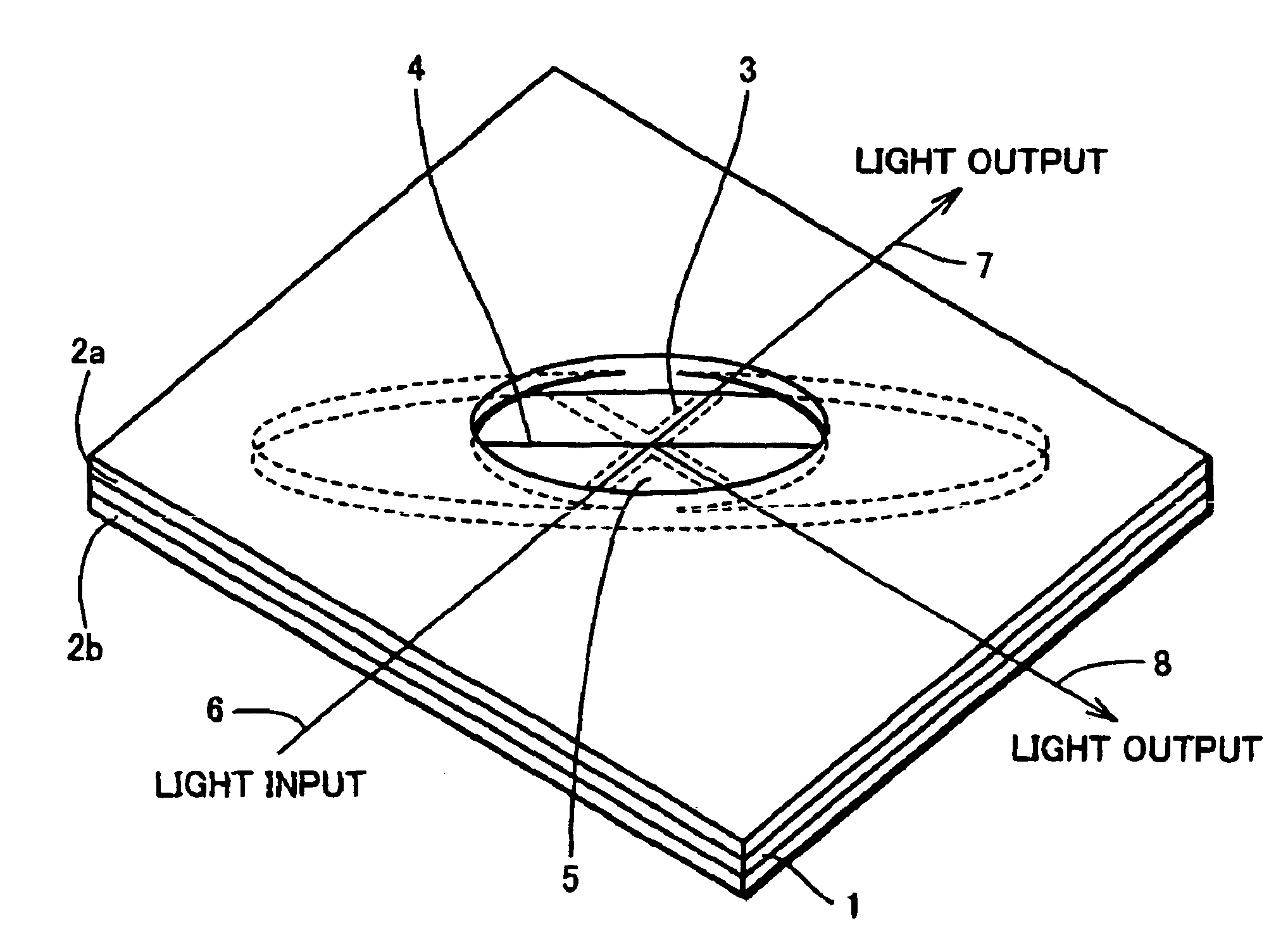
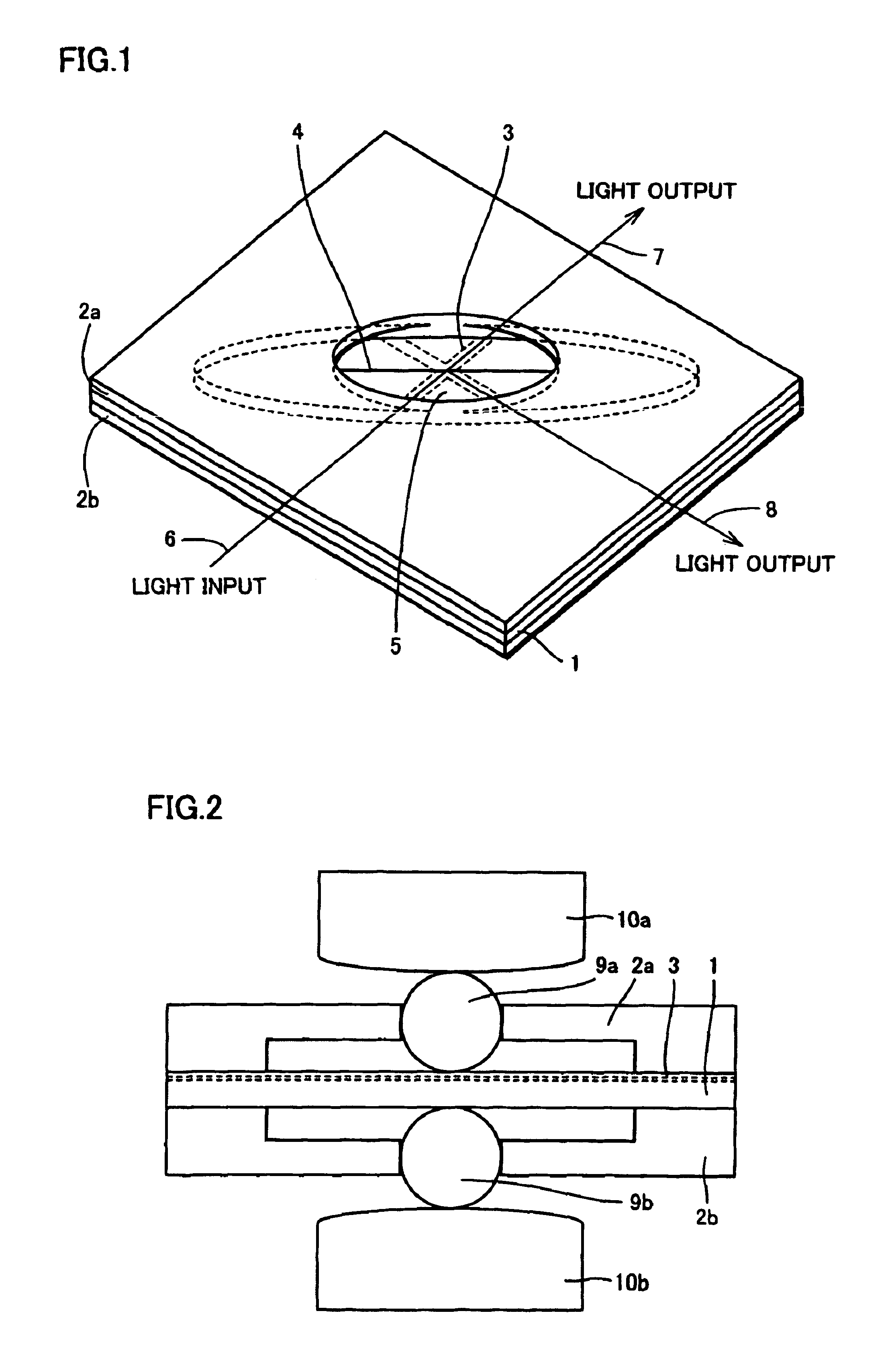
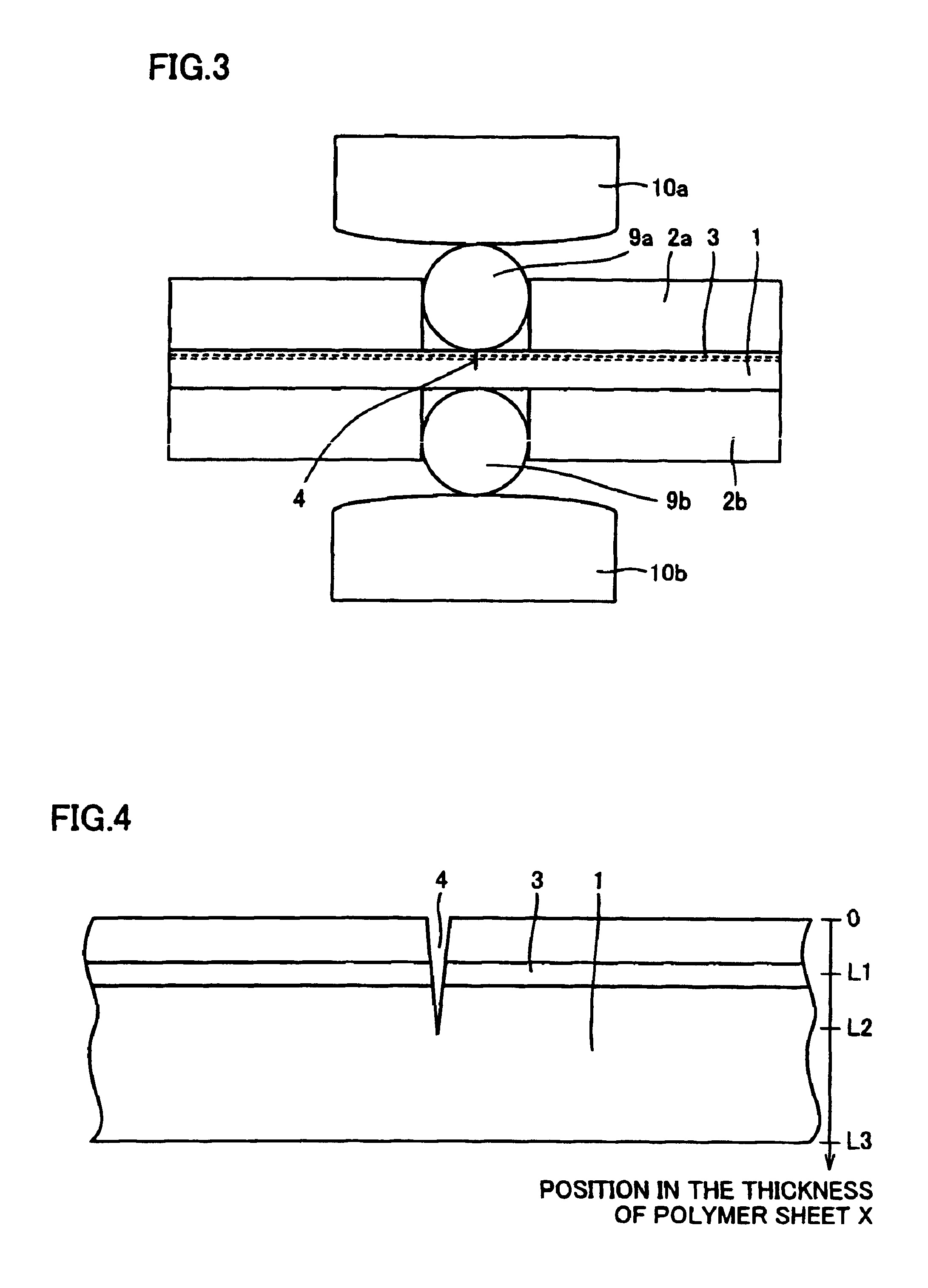
Referring to FIGS. 1 to 3, an optical switch according to a first embodiment of the present invention will be described. It should be noted that FIGS. 1 to 3 are enlarged views illustrating only one of the ports, while an optical switch in practical use includes multiple array of such ports on a plane.

An optical switch of the present embodiment is formed by holding a polymer sheet 1 between keep plates 2a and 2b. Optical waveguides 3 are arranged in the polymer sheet 1 crossing with each other, and a notch 4 is provided from one surface of the polymer sheet 1 such that it traverses the intersection of the optical waveguides 3. An optical signal enters the optical waveguides 3 from the lower left side of FIG. 1 as an incident light 6, then goes out from one side as a transmitting light 7 when transmitting through the notch 4 as such, and goes out from another side as a reflecting light 8 when reflected by the notch 4. An openings 5 of two keep plates 2a and 2b are circular as viewed ...

second embodiment

Referring to FIGS. 7 to 9, an optical switch according to a second embodiment of the present invention will be described. It should be noted that FIG. 7 is an enlarged view of only one of the ports, while an optical switch in practical use includes multiple array of such ports on a plane. Additionally, one keep plate in contact with the upper surface of a polymer sheet 1 is not shown in FIG. 7.

As a direct pushing member, a ball 9 is employed also in the present optical switch. A keep plate 2e is in contact with bottom of the polymer sheet 1, and a stopper plate 14 is in contact with bottom of the keep plate 2e. As shown in FIG. 8, the keep plate 2e has a tapered hole 17 tapered off upward, and therefrom a slit is extending in two directions forming an angle of approximately 180° with each other. As shown in FIG. 9, a stopper plate 14 is provided with a ball receiving hole 18 having a diameter smaller than that of the ball 9. As shown in FIG. 7, the ball 9 is accommodated in the tape...

third embodiment

Referring to FIGS. 10 to 12, an optical switch according to a third embodiment of the present invention will be described. It should be noted that FIG. 10 is an enlarged view of only one of the ports, while an optical switch in practical use includes multiple array of such ports on a plane. Additionally, one keep plate in contact with the upper surface of a polymer sheet 1 is not shown in FIG. 10.

As a direct pushing member, a ball 9 is also employed in the present optical switch. A keep plate 2f is in contact with bottom of the polymer sheet 1, and a stopper plate 14n is in contact with bottom of the keep plate 2f. As shown in FIG. 11, the keep plate 2f has a tapered slit 19 tapered off upward. As shown in FIG. 12, a stopper plate 14n is provided with a ball receiving hole 18n in which a straight portion having a diameter slightly larger than that of the ball 9 and a tapered portion tapered off downward are connected. As shown in FIG. 10, the ball 9 is accommodated in a space, suppo...


PUM


Abstract

An optical switch includes a polymer sheet having an optical waveguide extending linearly therein, keep plates holding the polymer sheet therebetween, and driving means. The polymer sheet has a notch provided to traverse the optical waveguides, and the keep plates each have an opening at a position corresponding to the notch. The opening has an elongated shape along the extending direction of the notch at least on a surface of the keep plate in contact with the polymer sheet. The driving means is for selecting a course of light by switching open and closed states of the notch by pushing and not pushing the polymer sheet via the opening.

Description

BACKGROUND OF THE INVENTION1. Field of the InventionThe present invention relates to an optical switch employed for switching optical paths in an optical communication system and a method of manufacturing the same.2. Description of the Background ArtA conventional optical switch 90 will be described with reference to FIG. 21. This optical switch 90 is one shown in TuM1 (J. E. Fouquet, “Compact optical cross-connect switch based on total internal reflection in a fluid-containing planner lightwave circuit”) at OFC 2000 (Optical Fiber communication Conference, Mar. 7, 2000). Optical switch 90 is formed by a silica planar optical circuit substrate 51, where a two-dimensional optical circuit is formed by providing a rectangular optical waveguide having a slightly high refractive index within silica planar optical circuit substrate 51. Generally, silica planar optical circuit substrate 51 having a refractive index of about 1.5 is employed, while optical waveguide 91 portion is made of a m...

Claims


Application Information

Patent Timeline
IPC IPC(8): G02B6/12G02B6/35G02B26/08
CPCG02B6/12G02B6/3502G02B6/3538G02B6/3578G02B6/355G02B6/3574G02B6/3546
Inventor HATTA, TATSUOTABATA, SEIICHIRO
Owner MITSUBISHI ELECTRIC CORP
Why Eureka
Try Eureka